Multi-Tile Synchronization Using AMD RFSoC Device
This example shows how to implement and use multi-tile synchronization (MTS) using an RF Data Converter block on an RFSoC device to resolve the time alignment issue of multiple channels across different tiles on an RFSoC device. The RFSoC devices have multiple channels of DAC and ADC across different tiles. This enables you to design complex communication systems that require MTS. In this example, you simulate a model that contains an RF Data Converter block with two DAC and ADC channels in the MTS configuration. You can also observe the effect of the RF Data Converter MTS on two-channel signals, aligning both channels together even though they reside in different tiles post-MTS.
Supported Hardware Platforms
AMD® Zynq® UltraScale+™ RFSoC ZCU111 Evaluation Kit + XM500 balun card + DC blocks
AMD Zynq UltraScale+ RFSoC ZCU216 Evaluation Kit + XM655 balun card + DC blocks
AMD Zynq UltraScale+ RFSoC ZCU208 Evaluation Kit + XM655 balun card + DC blocks
Design Task and System Specifications
Consider an RF application that requires phase synchronization among multiple channels. For example, transmitting signals from an antenna array with a particular phase and amplitude is important to form the beam in a particular direction. Transmitting chains contain different nonlinear components and different PLLs, which produce random phase shifts in the transmitting signals. Hence, different transmitting paths must be synchronized to transmit signals with the phase shift. Phase synchronization plays a vital role in such applications. MTS is an important capability of the RFSoC device that enables beamforming, phased array RADAR, massive MIMO, and more.
In this example, the design task involves creating an FPGA algorithm that generates sinusoidal tones for all eight DAC channels of the RF Data Converter block. The output from these DACs is looped back to the ADC input for processing on the FPGA. The FPGA then captures ADC samples from two channels and sends them to the processor for visualizing the MTS between any two ADC channels. The following specifications outline the requirements for the MTS mode.
MTS for AMD Zynq UltraScale+ RFSoC ZCU111, ZCU216, and ZCU208 evaluation kits requires specific sample rates. The SYSREF signals from an external clock satisfy these sample rates. The SYSREF frequency must meet the following requirements. For more information, see PG269 on the AMD website.
If synchronizing ADC and DAC tiles with different sample frequencies, the frequency must be an integer submultiple of GCD (DAC sample rate/16, ADC sample rate/16).
SYSREF frequency must also be an integer submultiple of all PL clocks. This is to ensure the periodic SYSREF signal is always sampled synchronously.
SYSREF frequency must be less than 10 MHz.
For ZCU111, ZCU216, and ZCU208 boards, the reference clock must be an integer multiple of the SYSREF frequency. For the ZCU111 board, the default SYSREF frequency produced by the LMK is 7.68 MHz. To meet the requirements, choose a sampling rate from the frequencies available in the LMK that is a multiple of 7.68 MHz.
Select the reference clock to meet the SYSREF requirement. For instance, when using ZCU208 and ZCU216 boards, select a frequency of 245.76 MHz. However, for the ZCU111 board, the design utilizes an external phase-locked loop (PLL) reference clock instead of the internal clock for MTS mode. Based on these requirements, the ADC and DAC sample rate in this example is 1966.08 mega-samples per second (MSPS).
Use a Vivado® version that corresponds to the PetaLinux version of the RFSoC device you use for best results.
Design Using SoC Blockset
Use an SoC model as the top model. For this example, use the soc_mts_zcu111_top as the top model with the Xilinx Zynq Ultrascale+ RFSoC ZCU111 Evaluation Kit hardware board. This model includes the FPGA model soc_mts_fpga and the processor model soc_mts_proc, which are instantiated as model references. The top model also includes the AXI4-Stream to Software block, which shares the external memory between the FPGA and the processor.
open_system('soc_mts_zcu111_top')
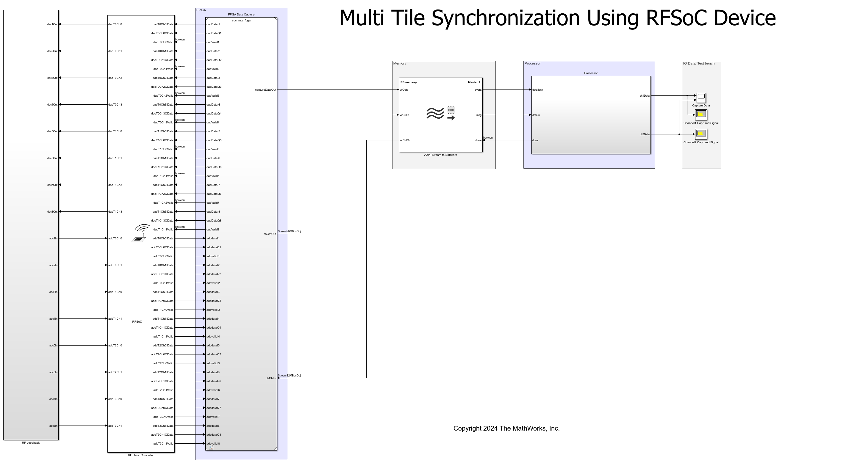
close_system('soc_mts_zcu111_top')
RF Data Converter Configuration
An RFSoC device has its RF data converter connected to the programmable logic. To configure the ADC and DAC settings, use the RF Data Converter block. The block provides an interface to the AMD RF Data Converter IP in Simulink® for modeling a wireless system implemented on an AMD RFSoC device.
To meet the system requirement of 1966.08 MSPS as the data rate for DACs and ADCs, you must choose the values of the Interpolation mode, Decimation mode, and Samples per clock cycle parameters such that the effective clock cycle (sample rate) for the wireless algorithm FPGA is in the desirable range. The parameter values are displayed on the block as Stream clock frequency after you click Apply.
For this example, in the DAC tab, set Interpolation mode to 8 and Samples per clock cycle to 2. In the ADC tab, set Decimation mode to 8 and Samples per clock cycle to 2. In the DAC and ADC tabs, set NCO frequency (GHz) to 0. These values imply a Stream clock frequency value of 1966.08/(8*2) = 122.88 MHz. In the Advanced tab, select the Multi tile sync option for MTS.

Hardware Logic Design
The FPGA model soc_mts_fpga contains two subsystems: DAC Tone Generation, which is connected to the DAC portion of the RF Data Converter block, and ADC Capture, which is connected to the ADC portion. The FPGA model is configured so that the DAC tiles do not produce output until the TxStreamEnable signal is asserted. This delay gives the RF Data Converter additional time to complete any required synchronization. Open the DAC Tone Generation subsystem to see how the model gates the TxStreamEnable signal based on data transmission.
open_system('soc_mts_fpga')
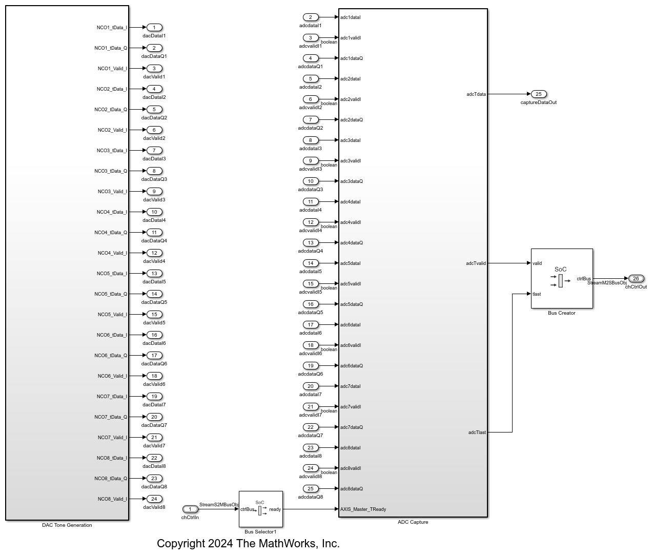
close_system('soc_mts_fpga')
In the DAC Tone Generation subsystem, two consecutive samples of the sinusoid waveform are generated in parallel by using two NCO blocks. Each NCO block has a different offset. The two samples comprise 32 bits of data.
The ADC Capture subsystem incorporates trigger and capture logic to acquire ADC RF samples and store them in a FIFO. This subsystem includes ADC channel selection subsystems to choose the specific ADC channels for capture, as well as a Trigger Capture subsystem responsible for initiating and capturing the samples. The Trigger Capture subsystem then reads the captured data and transmits it to the processor to visualize the acquired signal.
Processor Logic Design
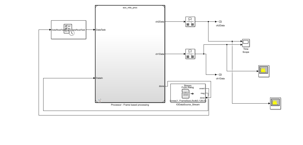
The processor logic contains an event-based task driven by the arrival of data from the FPGA through the DDR memory. The processor algorithm task is denoted as dataTask in the Task Manager block and is specified as event driven. The Task Manager block schedules data asynchronously by means of the buffer-ready event rdEvent in the memory, denoting the arrival of a frame of data from the FPGA. The algorithm itself is modeled under the Processor Algorithm Wrapper subsystem in the processor model soc_mts_proc and connected to the Task Manager block at the top level. To operate on the data received as a frame of two packed samples of two ADC channels with the fixdt(0,128,0) data type, you must first unpack and restore the signedness of each channel's data. The output of the Processor Algorithm Wrapper subsystem is then connected to the Spectrums and Time scope with two channels for visualization. In a separate Initialize Function subsystem, various registers on the FPGA subsystems are initialized with their default values.
open_system('soc_mts_proc')
close_system('soc_mts_proc')
Simulate
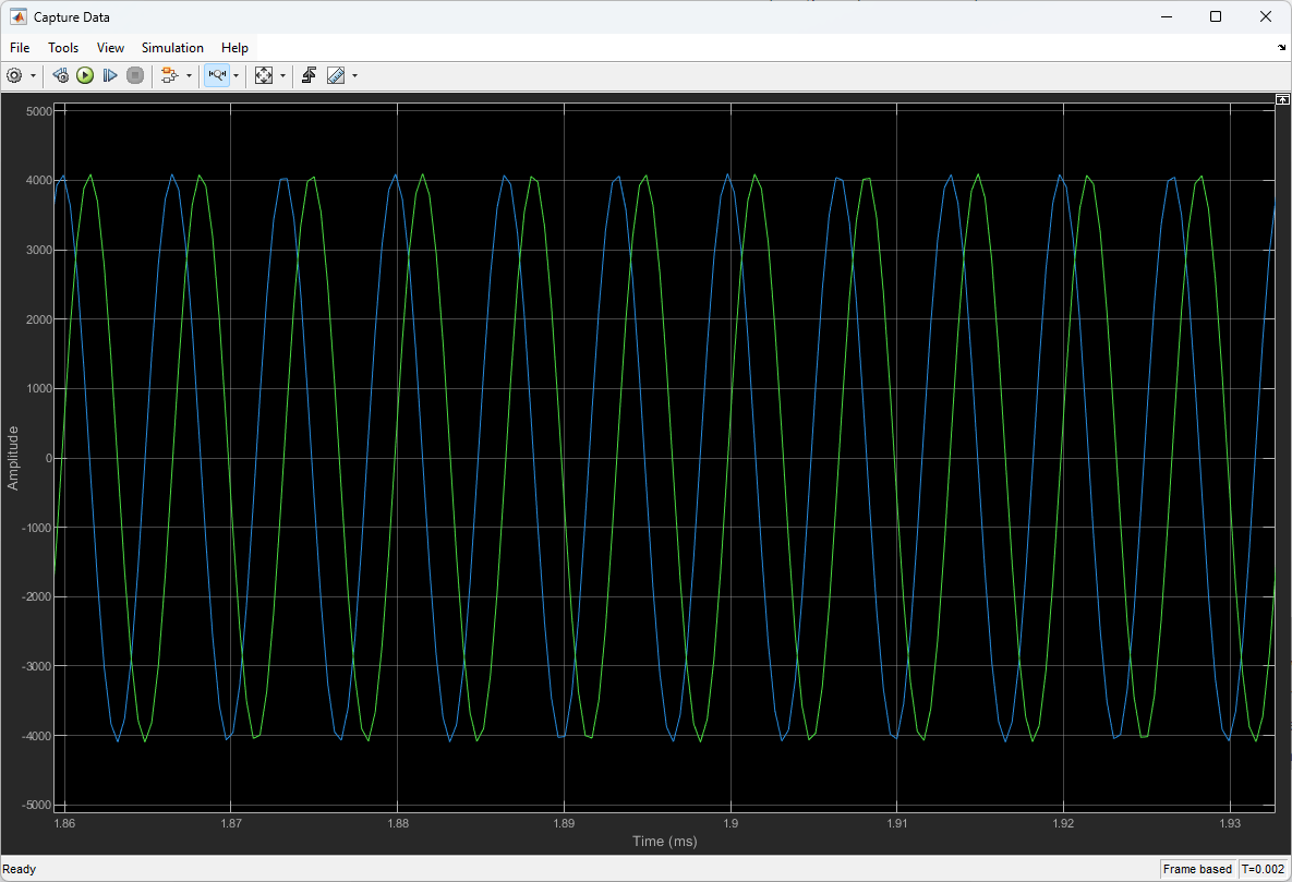
Upon running the model, the sinusoidal tone generated by the FPGA is routed back from the FPGA through the RF Data Converter block to the processor. The FPGA's ADC Capture subsystem captures this waveform. In the processor system, the waveforms are analyzed in the frequency domain using Spectrum Scope blocks named Channel1 Captured Signal and Channel2 Captured Signal, corresponding to selected ADC channels for MTS. To assess phase synchronization effects, the waveforms are also visualized in the time domain using a Time Scope with two channels named Capture Data.
Implement and Run on Hardware
Hardware Setup
Connect the SMA connector on the XM500 balun card to complete the loopback between the DAC and ADC according to these connections.

To implement the model on a supported SoC board, use the SoC Builder tool. Ensure that the Hardware Board is set to Xilinx Zynq UltraScale+ RFSoC ZCU111 Evaluation Kit on the System on Chip tab of the Simulink toolstrip.
To open SoC Builder, click Configure, Build, & Deploy. After the SoC Builder tool opens, follow these steps.
On the Setup screen, select Build model. Click Next.
On the Select Build Action screen, select Build and load for external mode. Click Next.
On the Select Project Folder screen, specify the project folder. Click Next.
On the Review Hardware Mapping screen, click Next.
On the Review Memory Map screen, view the memory map by clicking View/Edit. Click Next.
On the Validate Model screen, check the compatibility of the model for implementation by clicking Validate. Click Next.
On the Build Model screen, begin building the model by clicking Build. An external shell opens when FPGA synthesis begins. Click Next.
On the Connect Hardware screen, test the connectivity of the host computer with the SoC board by clicking Test Connection. To go to the Run Application screen, click Next.
The FPGA synthesis can take more than 30 minutes to complete.
Click the Load button to load the generated bitstream and run the model on the SoC board.
Run Model in External Mode
After the bit file is loaded, open the generated software model.
Run the model in external mode by clicking Monitor & Tune. You can control the configuration from the Simulink model. Copy the spectrum analyzers and time scope from the top model and connect to the rate transition blocks as shown in this figure, and run the model. You can observe the received signal waveforms in time scope and observe the phase synchronization of the two channels in MTS mode. You can change the adcChannelSelect1 and adcChannelSelect2 channel numbers to different channel numbers and observe the phase synchronization between the selected channels. It is better to choose differential channels for improved phase synchronization.

Run with Host IO Script
You can also verify the example model with the host I/O script. Run the soc_mts_zcu111_top_interface.m script (a modified version of the generated host interface script) and verify the results. It demonstrates near-perfect alignment between the channels.

Try Different Hardware Boards
To run the example on ZCU216 and ZCU208 hardware boards, use the soc_mts_zcu216_top and soc_mts_zcu208_top models, respectively. Change the hardware board in the soc_mts_proc model to the corresponding hardware board.
To target the ZCU216 board, set the hardware board in the
soc_mts_procmodel toXilinx Zynq UltraScale+ RFSoC ZCU216 Evaluation Kit.
To target the ZCU208 board, set the hardware board in the
soc_mts_procmodel toXilinx Zynq UltraScale+ RFSoC ZCU208 Evaluation Kit.
Repeat the steps from the Implement and Run on Hardware section.
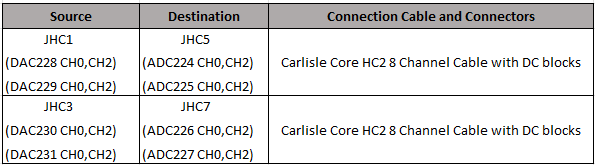
Hardware Setup for ZCU216 and ZCU208
Connect the XM655 balun card and complete the loopback between the DACs and ADCs shown in the table. You receive two Carlisle Core HC2 8 Channel cables with the kit, allowing you to loop back only four channels. If you need to loop back all eight channels, you require two additional Carlisle Core HC2 8 Channel cables.
Configure Digital Local Oscillator
While running MTS, you must not change the digital local oscillator (LO) frequency on the RFSoC. The LO of each channel may not be time-aligned, which can cause misalignment between channels. The RFSoC provides ways to address this by synchronizing the reset condition on all channels based on tile events. By configuring the tile events to respond to a SYSREF signal, you can achieve time alignment when using the mixer and LO frequency during MTS.
In this example, RF Data Converter parameter NCO frequency (GHz) is set to 0 to avoid LO alignment issues from affecting the direct cable loopback. To modify the LO frequency, first disable SYSREF capture, make the necessary changes to the LO frequency, and then re-enable SYSREF.
The example provides scripts that demonstrate this process:
soc_zcu111_changeLO.mfor the ZCU111 boardsoc_zcu216_changeLO.mfor the ZCU216 boardsoc_zcu208_changeLO.mfor the ZCU208 board
Run the script corresponding to your board to adjust the LO frequency.
MTS Configuration for Non-Loopback Applications
When you configure MTS for a direct cable loopback, the data channels are well aligned without accounting for the channel latency. For applications other than direct cable loopback, you must consider channel latency to achieve better synchronization.
To configure MTS with channel latency, follow these steps:
1. Determine the latency of the channels on each tile by using the RFTool. Add the following commands in the RF_Init.cfg file located in the SD card at /mnt/hdlcoder_rd.
MTS_Sysref_Config 1 3 15
MultiConverter_Sync 1 -1 3
MultiConverter_Sync 0 -1 15
MTS_Sysref_Config 0 3 15
MTS_Sysref_Config uses one-hot decoding to control which tiles are enabled. These commands assume a configuration with two DAC tiles and four ADC tiles on the ZCU111 board. Passing 3 instructs the RFTool to configure the first two DAC tiles. Passing 15 instructs the RFTool to configure all four ADC tiles.
Reboot the board and observe the output captured in the rf_init.log file available on the SD card at /mnt/.
2. Calculate the target latency that you must set for the channels. Determine the target latency by adding an appropriate margin value to the latency value obtained in step 1. For more information on how to determine the target latency for the channels, see Deterministic Multi Tile Synchronization API Use on the AMD website.
DAC_Latency: "MultiConverter_Sync 1" return latency + margin
ADC_Latency: "MultiConverter_Sync 0" return latency + margin
3. Specify the target latency by adding the following commands into the RF_Init.cfg file located in the SD card at /mnt/hdlcoder_rd. Reboot the board to apply these settings.
MTS_Sysref_Config 1 3 15
MultiConverter_Sync 1 <DAC_Latency> 3
MultiConverter_Sync 0 <ADC_Latency> 15
Each time you power off the board, the target latency calculated in step 2 changes. The latency changes because the return latency obtained in step 1 can vary each time you power on the board.
Summary
This example shows how to design, implement, and use MTS using an RF Data Converter block on an RFSoC device to resolve the time alignment issue of multiple channels across different tiles on an RFSoC device using SoC Blockset. You can use this example as a reference for designing your application that requires phase synchronization between different channels.