QPSK Transmit and Receive Using Zynq and FMCOMMS2/3/4
This example shows how to simulate and deploy a quadrature phase-shift keying (QPSK) transmit and receive algorithm in Simulink® using an SoC Blockset™ implementation. You model a QPSK communication system that can transmit and recover information for a real-time system. You then implement the algorithms on an AMD® Zynq® ZC706 evaluation kit + Analog Devices® FMCOMMS2/3/4 card and a ZedBoard™ + Analog Devices FMCOMMS2/3/4 card.
QPSK Transmitter and Receiver Design
The design task is to build a wireless communication system with a QPSK transmitter and receiver, and then to implement the system on an AMD Zynq device. This figure gives an overview of the transmission and reception steps.
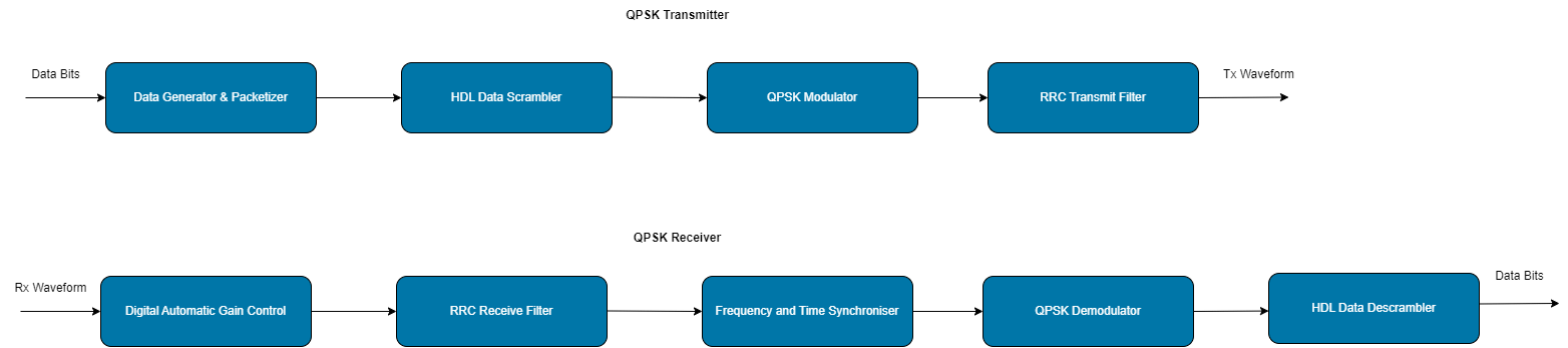
The QPSK transmitter samples the input at a bit rate equal to twice the symbol rate. The Data Generator & Packetizer step collects the data bits, generates the preamble bits, and forms the packet bits. The HDL Data Scrambler step scrambles the data bits of each packet to increase bit transitions and avoid long running sequences of the same bit. The QPSK Modulator step modulates the packet bits to generate QPSK symbols. The RRC Transmit Filter step upsamples and pulse-shapes the QPSK symbols to generate the transmission waveform at a sampling rate of four times that of the symbol rate.
The QPSK receiver samples the input at the transmission rate. The Digital Automatic Gain Control step adjusts the gain of the received waveform to attain the desired amplitude level. The RRC Receive Filter step performs matched filtering on the AGC output. The Frequency and Time Synchronizer step synchronizes the frequency and, and then generates QPSK symbols for each packet. The QPSK Demodulator step demodulates the QPSK symbols to generate packet bits. The HDL Data Descrambler step descrambles the packet data bits that stream out of the receiver.
Design QPSK Transmitter and Receiver
This figure shows a simplified functional block diagram of the model.

The soc_QPSK_top model is the top model. Set the hardware board to Zedboard. The top model includes the soc_QPSK_fpga FPGA model and the soc_QPSK_proc processor model as model references. The top model also includes AXI4-Stream to Software and AXI4-Software to Stream blocks, which share the external memory between the FPGA and the processor.
open_system("soc_QPSK_top")
![]()
Design Parameters - transfers data as a frame of samples from the FPGA to the processor across the shared memory.
These parameters affect the performance requirements.
Frame Size - Number of samples in a frame.
Number of Buffers - Number of frame buffers in memory channel. The FPGA algorithm continuously writes data as frame buffers into the memory. The processor then reads these frame buffers to execute the identification algorithm task.
The top model has these subsystems:
External I/O- AD9361 RF Input and Output blocks connect to each other using a simplified channel model.FPGA- FPGA algorithms as a model reference.Memory- Memory channel between the FPGA and the processor. It simulates the latencies in the HW/SW connection.Register Write- FPGA registers that the processor configures.Processor- Task Manager connected to processor model. The Task Manager controls the scheduling of processor tasks. The processor algorithm and initialization tasks are defined in a separate model. This subsystem includes this algorithm and these tasks using model references.
Hardware Logic Design
open_system("soc_QPSK_fpga")
![]()
In general, the model uses the programmable logic of the FPGA for high rate signal processing and the ARM for slower rate and control functionality. The user logic in FPGA programmable logic implements high-rate processing modules, a QPSK transmitter design, a channel, a QPSK receiver design, and a compute BER module. The FPGA programmable logic adds further control parameters and monitor signals to the FPGA IP core to adjust the design in real time and display the status of FPGA signals using AXI-Lite registers, which you can access by using a processing system. The ARM processing system pulls the status signal information from the FPGA and displays the information on the host.
The AXI4-Lite block has these ports:
externalDataActive - Switch messages from an internal LUT to an external message.
overAir - Switch the data flow over the air to a loopback between the QPSK Tx and QPSK Rx blocks via a channel inside the FPGA.
insert CFO - Sets the value of carrier frequency offset (CFO) to add to the waveform in the channel.
insert CPO - Sets the value of carrier phase offset (CPO) to add to the waveform in the channel.
rstCS - Resets the carrier synchronizer in the QPSK receiver.
bitErrors - Streams the number of bit errors from the QPSK receiver.
bitReceived - Streams the number of bits received from the QPSK receiver.
numOfFramesSynced - Streams out the number of frames synchronized.
estimatedCoarseCFO - Streams out the estimated coarse CFO.
Processor Logic Design
The processor logic contains read and write tasks. The model displays status information such as the number of synchronized frames, estimated CFO, number of received bits, and number of bit errors from the QPSK receiver. The controller provides the constellation data, decoded message, transmitted message, and status information to the MATLAB host using UDP blocks.
These event-based reading tasks are driven by the arrival of data from the FPGA through the DDR memory.
TxMsg Read Event - Relays the transmitted message to the host over the UDP protocol.
Decoded Msg Read Event - Relays the decoded message to the host over the UDP protocol.
Constellation Read Event - Relays the constellation and status signals to the host over the UDP protocol.
TxMsg Write Event - Relays the external message from the processor to the FPGA fabric through the DDR memory.
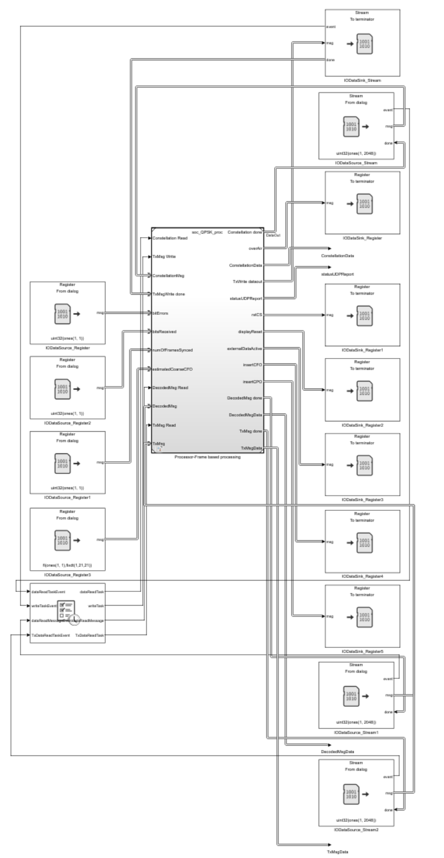
The Processor Algorithm Wrapper subsystem in the soc_QPSK_proc subsystem models these tasks, which connect to the Task Manager block at the top level.
open_system("soc_QPSK_proc")
![]()
The Initialize Function subsystem initializes appropriate hardware configuration registers. The AD9361 blocks set the center frequency, gain mode, and baseband sampling rate of the attached FMC RF board.
Host Model
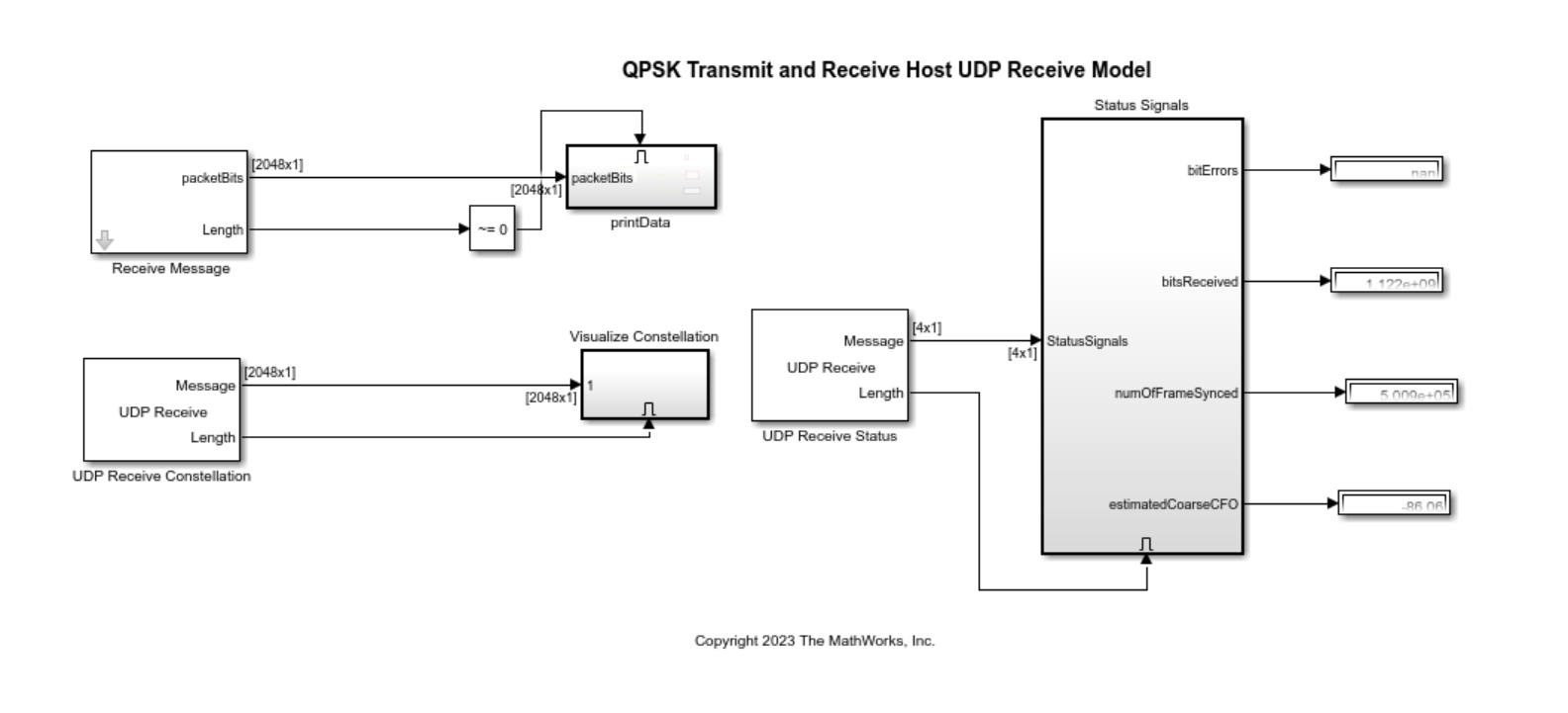
The processor sends the QPSK Receiver block outputs, data, and receiver status signals directly back to the host over the Ethernet link using UDP Write blocks. The IP address of the UDP Write block in the processor model must be the IP address of the host. This interface model, which runs on the host, receives data from the hardware platform then preprocesses.
open_system("soc_QPSK_hostUDPReceive")
![]()
Simulate QPSK Transmission and Reception
Because the HDL-optimized blocks in the model need sample-based signal simulation, the simulation takes a few minutes to complete. This figure shows the constellation diagram and decoded message from the simulation.


Implement and Run on Hardware
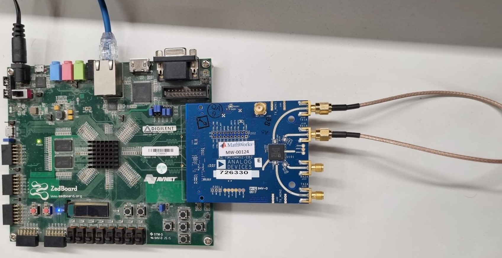
Hardware Setup
Connect the SMA cables with the FMCOMMS card on the Zedboard to complete the loopback between the transmitter and the receiver.
To implement the model on a supported SoC board, use the SoC Builder tool. Set the Hardware Board option to Zedboard on the System on Chip tab of the Simulink Toolstrip.

For targeting, invoke hdlsetuptoolpath to set up the synthesis tool.
hdlsetuptoolpath('ToolName','Xilinx Vivado',...
           'ToolPath','C:\Xilinx\Vivado\2022.1\bin\vivado.bat');
To open SoC Builder, click Configure, Build, & Deploy. After the SoC Builder tool opens, follow these steps.
1) On the Setup screen, select Build Model and click Next.
2) On the Select Build Action screen, select Build, load and run.
3) On the Select Project Folder screen, specify the project folder and then click Next.
4) On the Review Hardware Mapping screen, click View/Edit... to view the pin mapping, module assignment for peripheral devices and then click Next.
5) On the Review Memory Map screen, click View/Edit... to view the memory map and then click Next.
6) On the Validate Model screen, click Validate to check the compatibility of the model for implementation and then click Next.
7) On the Build Model screen, click Build to begin building the model. An external shell opens when FPGA synthesis begins.
8) On the Connect Hardware screen, click Test Connection to test the connectivity of the host computer with the SoC board. Click Next to go to the Run Application screen.
To run this example using the provided pregenerated bitstream,
first close the external shell to terminate FPGA synthesis.
Then, copy the pregenerated bitstream to your project folder.
copyfile(fullfile(matlabshared.supportpkg.getSupportPackageRoot, ...
 "toolbox","soc","supportpackages","xilinxsoc","xilinxsocexamples", ...
 "bitstreams","soc_QPSK_top-zedboard.bit"),"./soc_prj");
Click Load and Run to load the pregenerated bitstream and run the model on the SoC board. Open the generated software model after the bit file loads.
To implement the model on a ZC706 board, you must first configure the model for the AMD Zynq ZC706 evaluation kit and set the hardware implementation by following these steps.
1) In the Simulink toolstrip, on the System on Chip tab, open the Configuration Parameters window by clicking Hardware Settings.
2) In the Configuration Parameters window, in Hardware Implementation,select Xilinx Zynq ZC706 evaluation kit from Hardware board drop-down list on both top and processor model.
Next, open SoC Builder and follow the same steps as for the Zedboard Modify the copyfile command to match the soc_QPSK_top_zc706 bitstream with the .bit extension
To run the model in external mode open the generated soc_QPSK_top_sw software interface model by entering this command in the MATLAB Command Window: open_system("soc_QPSK_top_sw")
You can control the configuration from the Simulink model by clicking Monitor & Tune.
Constellation and Status Signals from Hardware
Plot Results
Toggle the switch linked to the externalDataActive port to switch sourcing data between the LUT message on the FPGA and the ARM-based external message from the soc_QPSK_top_sw model. These figures show the decoded message and constellations when you transmit a waveform over the air. The diagnostic viewer displays the decoded message.
Constellation Plot
Host UDP Model - Internal LUT Message:
Host UDP Model - External Message:
See Also
Blocks
- Software to AXI4-Stream | AXI4-Stream to Software | Register Channel | Register Write | Stream Read | Task Manager | UDP Read (HOST) | UDP Write