RFSoC Template
The RFSoC template provides a simulation model for an SoC reference design available from SoC Blockset™ Support Package for AMD FPGA and SoC Devices. Use this template to simulate the full reference design. Analyze the effects of internal and external connectivity on transmit and receive communication algorithms, such as memory behavior and Radio Frequency (RF) input/output (I/O) behavior.
To get started with the SoC Blockset model for designing an RFSoC-enabled wireless communication system, follow the steps in Create SoC Model Using SoC Blockset Template. Then, add your transmitter and receiver algorithms in the FPGA subsystem and your processor algorithm in the Processor subsystem.

Required Products
DSP System Toolbox™
SoC Blockset Support Package for AMD FPGA and SoC Devices
Template Structure
The RFSoC template comprises three models: the Top model, the FPGA model, and the
Processor model. In the Top model, the RF Data Converter block connects
to the FPGA block and provides an RF I/O interface. The FPGA block implements receiver
and transmitter algorithms. The FPGA algorithm includes a Test Source
block, which generates a sinusoidal signal and drives it to the digital-to-analog
converter (DAC) through the Transmitter Algorithm subsystem. The Transmitter Algorithm
subsystem is implemented as simple pass-through wires, and the Receiver Algorithm
subsystem is implemented using down-sampler logic. The configuration register
SrcSelReg is modeled in the FPGA to select the data source for
the Receiver Algorithm subsystem. The processor writes the
SrcSelReg register to select either the test source from the
FPGA or the RF data from the analog-to-digital converter (ADC) in the RF Data
Converter block. Data from the FPGA subsystem is passed to the Processor
subsystem through a Memory Channel
block. The Channel Type parameter in the Memory
Channel block is set to AXI4-Stream to software via
DMA, which models the direct memory access (DMA) data transfer through
shared external memory.
Use this template as a guide, replacing the Receiver Algorithm and Transmitter Algorithm subsystems in the FPGA model and the Processor Algorithm subsystem in the Processor model with your own functionality. In this template, the RF Data Converter block is configured with a custom RF interface that has one DAC (DAC7) and one ADC (ADC1) and an I/Q digital interface. The number of samples per clock cycle is set to 2. The RF path in this template is looped back. If you want to use different data for the transmitter and receiver, you can remove the loop back and can provide your desired input data to the ADC.
The processor reads the computed data from the memory and performs additional computing (implemented in the template as a pass-through wire). You can view the simulation results by double-clicking the Time Scope block in the Testbench Sink subsystem.
Modify Project
Modify the FPGA Model
In the MATLAB® Toolstrip, on the Project Shortcuts tab, click Open FPGA model. Then, open the FPGA Tx-Rx Alg Wrapper subsystem. Three areas are highlighted in green, as shown in this figure. These areas represent user code and are located in the Test Source block, the Transmitter Algorithm subsystem, and the Receiver Algorithm subsystem.

The FPGA model includes these sections (highlighted in green) for you to modify.
Test Source block – This block generates a 500 kHz sinusoidal signal and drives it to the Transmitter algorithm subsystem. Modify the test source to your needs or replace it with an alternative source block.
Transmitter Algorithm subsystem – Contains Tx Algorithm subsystem highlighted in green. Replace the Tx Algorithm subsystem with your own transmitter algorithm.
Receiver Algorithm subsystem – Contains Rx Algorithm subsystem highlighted in green. Replace the Rx Algorithm subsystem with your own receiver algorithm.
IP Core Register Read blocks – Inside the design under test (DUT), add these blocks to add registers to your algorithm IPs. Initialize this block using a corresponding Register Write block in the Processor model.
To enable consistent simulation behavior, on the Project Shortcuts tab, click Open FPGA model and repeat this step.
Modify the Processor Model
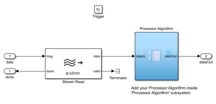
In the MATLAB Toolstrip, on the Project Shortcuts tab, click Open Processor model. The Processor model contains the Processor Algorithm Wrapper and the Initialize Function subsystems. The Processor Algorithm Wrapper subsystem is highlighted in blue, which represents the user code for the processor algorithm. Open the Processor Algorithm Wrapper subsystem and replace the internal Processor Algorithm subsystem (also highlighted in blue) with your desired algorithm. Open the Initialize Function subsystem and add a Register Write block for each IP Core Register Read block added in the FPGA model.

See Also
Use Template to Create SoC Model