SDR Template
The software defined radio (SDR) template provides a simulation model for an SoC reference design available from SoC Blockset™ Support Package for AMD FPGA and SoC Devices. Use this template to simulate the full reference design and analyze the effects of internal and external connectivity on and SDR algorithm, such as memory behavior and Radio Frequency (RF) I/O behavior.
To get started with SoC Blockset model for designing an SDR system, follow the steps to Create SoC Model Using SoC Blockset Template.

Required Products
Communications Toolbox™
SoC Blockset Support Package for AMD FPGA and SoC Devices
Template Structure
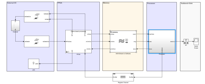
This template models an SDR transceiver composed of AD9361 transmitter and receiver blocks. The transceiver connects an RF channel to the FPGA, which implements a receiver and a transmitter algorithm. The FPGA algorithm includes a Test Source block, which generates a sinusoid signal and drives it to the transmitter. The FPGA algorithm also includes a Tx algorithm, implemented as simple pass-through wires, and an Rx algorithm, implemented as a gain block. A configuration register srcSel is modeled in the FPGA to select the source of data for the Rx algorithm. The processor writes the srcSel register to select either the test source from the FPGA or RF data from the transceiver. This register is modeled using the Register Channel block. Data from the FPGA algorithm is passed to the processor through a Memory Channel block.
Use this template as a guide and replace the Rx Algorithm and Tx Algorithm in the FPGA
and the Processor Algorithm in the processor with your own functionality. The memory
Channel Type parameter is set to AXI4-Stream to
software via DMA, which models the direct memory access (DMA) data
transfer through shared external memory.
The processor reads the computed data from the memory, and performs additional computing (implemented in the template as a pass-through wire). You can view the simulation results by double-clicking the Vector Scope block in the testbench sink.
Modify Project
Modify the FPGA Model
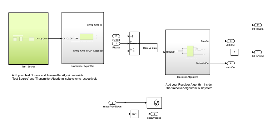
In MATLAB®, on the Project Shortcuts tab, click Open FPGA sample model. Then, open the FPGA Tx-Rx Alg Wrapper. Notice three areas highlighted in green. These areas represent user code and are located in the Receiver Algorithm block, in the Transmitter Algorithm block, and the Test Source block.

The FPGA model includes the following sections for you to modify (highlighted in green):
Test Source block – This block generates a 10-kHz sinusoid signal and drives it to the transmitter algorithm. Modify the test source to your needs or replace it with an alternative source block.
Receiver Algorithm subsystem – Inside the green-highlighted subsystem named Rx Algorithm, there is a block labeled Algorithm. The algorithm takes I/Q data as input and output with a valid signal. Replace this block with your own Rx algorithm.
Transmitter Algorithm – Inside the green-highlighted subsystem named Tx Algorithm, the algorithm has an input from the test source and two output signals: one to the RF channel and one to the FPGA. Replace this block with your own Tx algorithm.
To enable consistent simulation behavior, in the Project Shortcuts tab, click Open FPGA frame model and repeat this step.
Modify the Processor Model
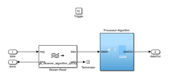
In MATLAB, on the Project Shortcuts tab, click Open processor model. The subsystem highlighted in blue represents the user code for the processor algorithm. Open the Processor Algorithm Wrapper and replace the internal Processor Algorithm block (also highlighted in blue) with your desired algorithm.

Modify the Register Channel
The top model of a template also includes a register channel to communicate between the processor and the FPGA model. Use the register channel to configure the FPGA model or to read and check status registers. The Register Channel block in the template includes one register. To add additional registers you must modify the register channel block parameters, the FPGA algorithm, and the processor algorithm:
Add registers to the register channel – Double-click the Register Channel block to open the block mask and add additional registers as needed. Adding registers creates additional ports on the Register Channel block. For additional information, see Register Channel.
Add ports to the processor model – Navigate to the Processor Algorithm Wrapper model. To navigate to the processor model, click Open Processor model on the Project Shortcuts tab. Double-click Processor Algorithm Wrapper to modify it.
For write registers, add an output port to the module and add logic to drive a value to the added output port. For read registers, add an input port and logic to process the information returned from a read register. From the top model, wire the port to the Register Channel block.
Add ports to the FPGA model – Navigate to the FPGA Algorithm Wrapper model. To navigate to the FPGA/Frame based processing model, click Open FPGA sample model on the Project Shortcuts tab. Double-click FPGA Algorithm Wrapper to modify it.
For write registers, add an input port to the module and logic to process the information returned from a read register. For read registers, add an output port and logic to drive a value to the added output port.
For equivalent behavior when using a Simulink® sample-based variant, repeat this step for the sample-based processing model in the FPGA wrapper.
From the top model, wire the new port to the Register Channel block.