Define PCB Antenna Layers
This step of the tutorial shows how to define the metal patch, dielectric, and ground plane layers in a PCB antenna using the PCB Antenna Designer app.
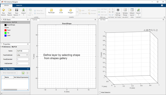
Open New Session
Type this command at the command line to open the PCB Antenna Designer app.
pcbAntennaDesigner

On the Design tab, click New Session to start a new session and open a blank canvas.
The default units for the canvas are millimeters (mm). The app uses global units. You can change the units by clicking the Canvas Settings button.
Define Board Shape
To design a PCB stack, you must first define a board shape. Select Rectangle from the Shapes section on the toolbar. Drag the shape on the canvas to create a rectangle.
Change the properties of Rectangle1 in the Properties pane to the following:
Center —
[0,0]Length —
25Width —
25

Add Ground Plane
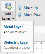
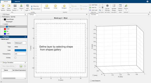
Click Add Layer on the toolbar and then select Metal Layer to add a metal layer.

The board shape is represented as a dotted line on the canvas.

Set the Name of the metal layer to GroundPlane.
Add Dielectric Layer
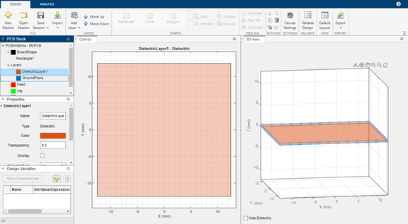
Click Add Layer on the toolbar and then select Dielectric Layer to add a dielectric layer DielectricLayer1.


Add Metal Patch Layer
Click Add Layer on the toolbar and then select Metal Layer to add a metal layer. Set the name of this layer to HNotchLayer.

Move Layers
You can move the layers using the Move Up and Move Down buttons on the toolbar.
