PCB Antenna Designer
Design, analyze, optimize, and export single or multifeed PCB antennas
Since R2021b
Description
The PCB Antenna Designer app lets you design and visualize single or multifeed PCB antennas.
Using this app, you can:
Create single-layer, multilayer metal, or metal-dielectric substrate PCB antennas.
Create an arbitrary number of feeds and vias in a PCB antenna.
Create shapes and perform Boolean operations.
Validate PCB antenna design.
Perform vector frequency analysis: impedance and S-parameters over a frequency range.
Perform scalar frequency analysis: current distribution, 3-D pattern and azimuth and elevation patterns.
Create variables for the object properties and optimize the design using these variables.
Generate mesh and estimate memory requirements.
Export your design to MATLAB® work space or script or, as Gerber files.

Open the PCB Antenna Designer App
MATLAB® Toolstrip: On the APPS tab, under RF AND MIXED-SIGNAL, click the PCB Antenna Designer app icon.
MATLAB command prompt: Enter
pcbAntennaDesigner.
Examples
Type this command at the command line to open the PCB Antenna Designer app.
pcbAntennaDesigner
On the Design tab click New Session to start a new session and open a blank canvas.
The default units for the canvas are in millimeters (mm). The app uses global units and you can change the units using the Canvas Settings button.
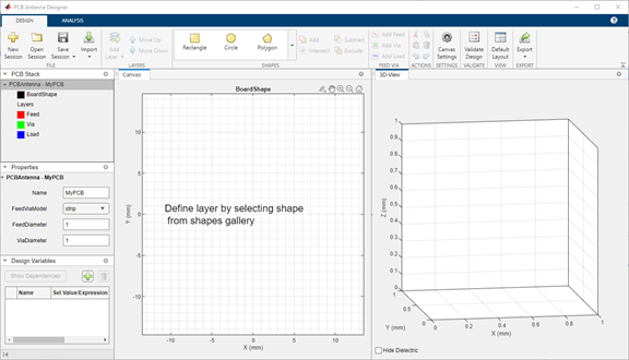
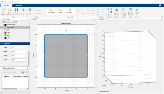
Define Board Shape
Select Rectangle from the Shapes section on the toolbar. Drag the shape on the canvas to create a rectangle and change the properties of Rectangle1 in the Properties pane to the following:
Center —
[0,0]Length —
20Width —
20
Add Ground Plane
Click Add Layer on the toolbar and then select Metal Layer. The shape of the board is represented as a dotted line on the canvas. Rename this layer to metalGround and then change the default color to [0.93 0.69 0.13].
The default metal type is PEC. To change the metal type, select Layers and then select a metal from the Type drop-down list. Use the default metal type for this example.

Select Rectangle from the Shapes section and drag the shape on the canvas to create a rectangular ground plane. Set the properties of the ground plane to the following
Name —
gndplaneCenter —
[0,0]Length —
20Width —
20

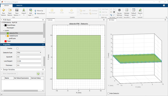
Add Dielectric Layer
Click Add Layer and then select Dielectric Layer to create a dielectric layer. A dielectric layer is created with the dimensions of the board shape. Set the properties of the layer to the following:
Name —
dielectricFR4DielectricType —
FR4Color —
[0.47 0.67 0.19]Transparency —
0.5Thickness —
0.6
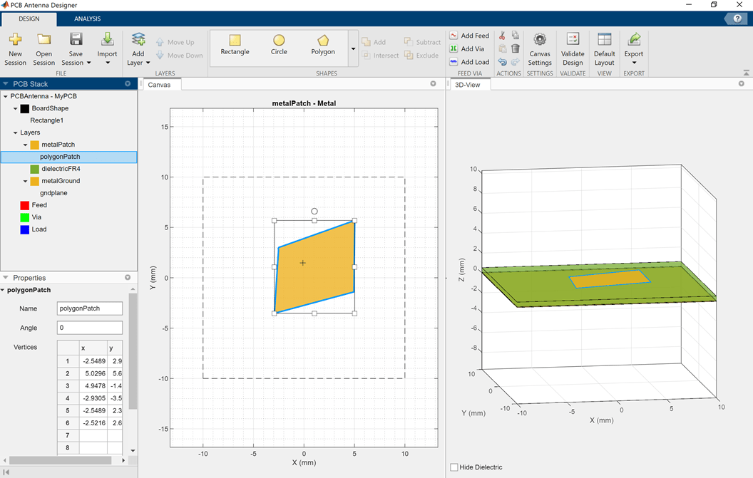
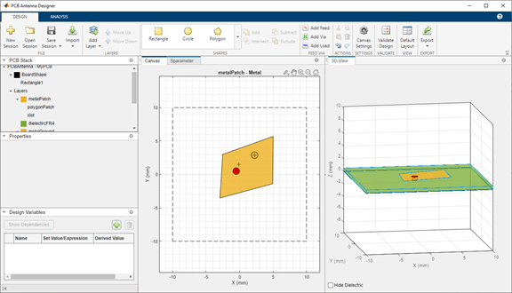
Create Polygon Patch
Click Add Layer and then select Metal Layer. Rename the metal layer to metalPatch.
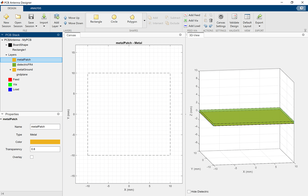
Select Polygon from the Shapes section. Select the vertices on the canvas to create a polygon patch. Set the properties of the polygon to the following:
Name —
polygonPatchAngle —
0
Under Vertices set the following values:
x1 = –2.5489 and y1 = 2.9902,x2 = 5.0296 and y2 = 5.6928,x3 = 4.9478 and y3 = –1.4050,x4 = –2.9305 and y4 = –3.5343,x5 = –2.5489 and y5 = 2.3623andx6 = –2.5216 and y1 = 2.6899
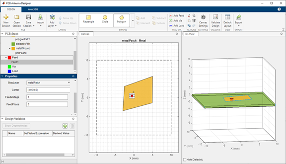
Add Feed
Click Add Feed from the Feed Via section on the toolbar. Set the properties of the feed to the following:
Name —
Feed1StartLayer —
metalGroundStopLayer —
metalPatchCenter —
[–0.5 0.5]
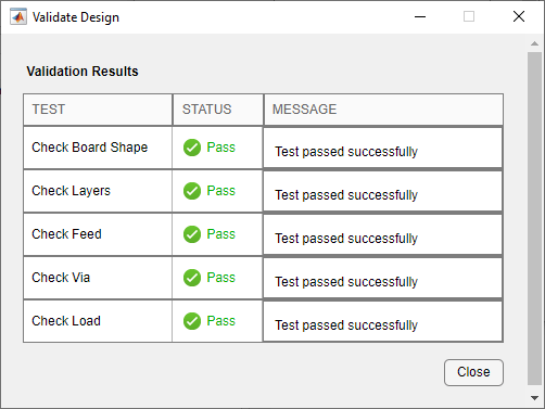
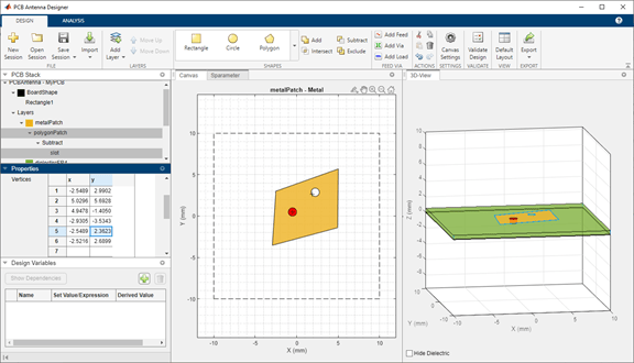
Validate Your Design
Click Validate Design on the toolbar to validate your board shape, layers, feed, via, and load.
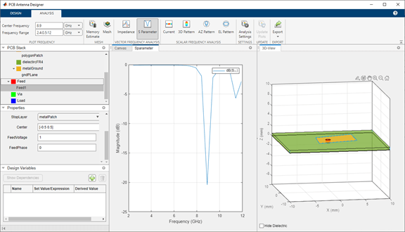
Analyze Your Design
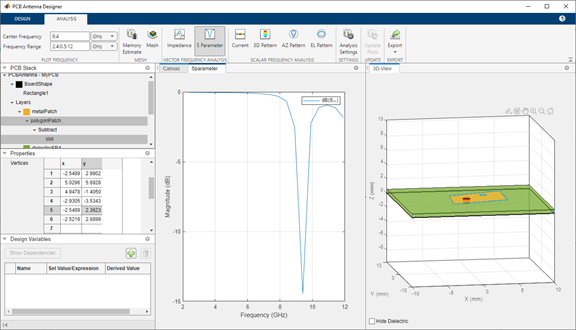
In the Analysis tab, set Center Frequency to 8.9 GHz and Frequency Range to 2.4:0.5:12 GHz. Click S-parameters under the Vector Frequency Analysis section to plot the reflection coefficient of the PCB patch antenna. The PCB patch antenna resonates at 8.9 GHz.
This example employs adding a slot to shift the resonant frequency. To add a circular slot, in the Design tab, select metalPatch and then select the Circle in the Shapes. Set the properties of the circle to the following:
Name —
slotCenter —
[2.24675 2.88105]Radius —
0.5
Select the polygonPatch and the slot you created in the previous step and then select Subtract on the toolbar.
In the Analysis tab, set Center Frequency to 9.4 GHz and click Update Plots. The PCB patch antenna now resonates at 9.4 GHz.
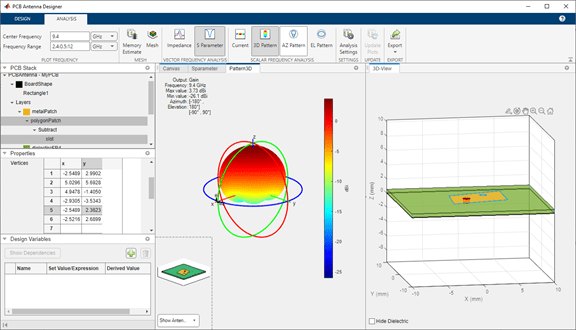
Click 3D Pattern in the Scalar Frequency Analysis section to plot the 3D radiation pattern. The directivity of the PCB patch antenna is 3.69 dBi.
This example uses a PCB patch antenna design from the Design and Analyze X-Band Custom PCB Patch Antenna example.
Follow the Design and Analyze X-Band Custom PCB Patch Antenna example to design a PCB patch antenna.
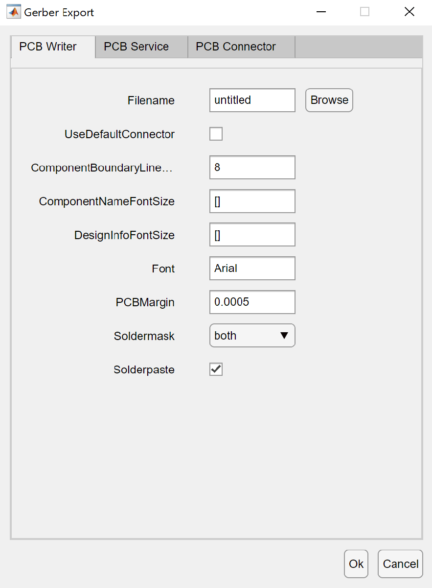
In the Analysis tab, click Export and then select Export as Gerber File. In the Gerber Export dialog, select Browse in the PCB Writer tab to select the directory in which you want the Gerber files to be stored. Clear the UseDefaultConnector.
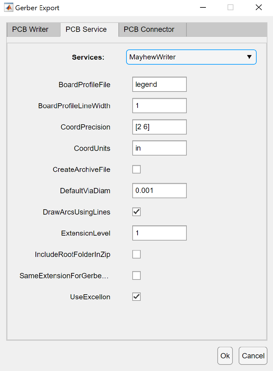
In the PCB Services tab, under Services, select MayhewWriter. The PCB writer uses the selected service to create the Gerber files.
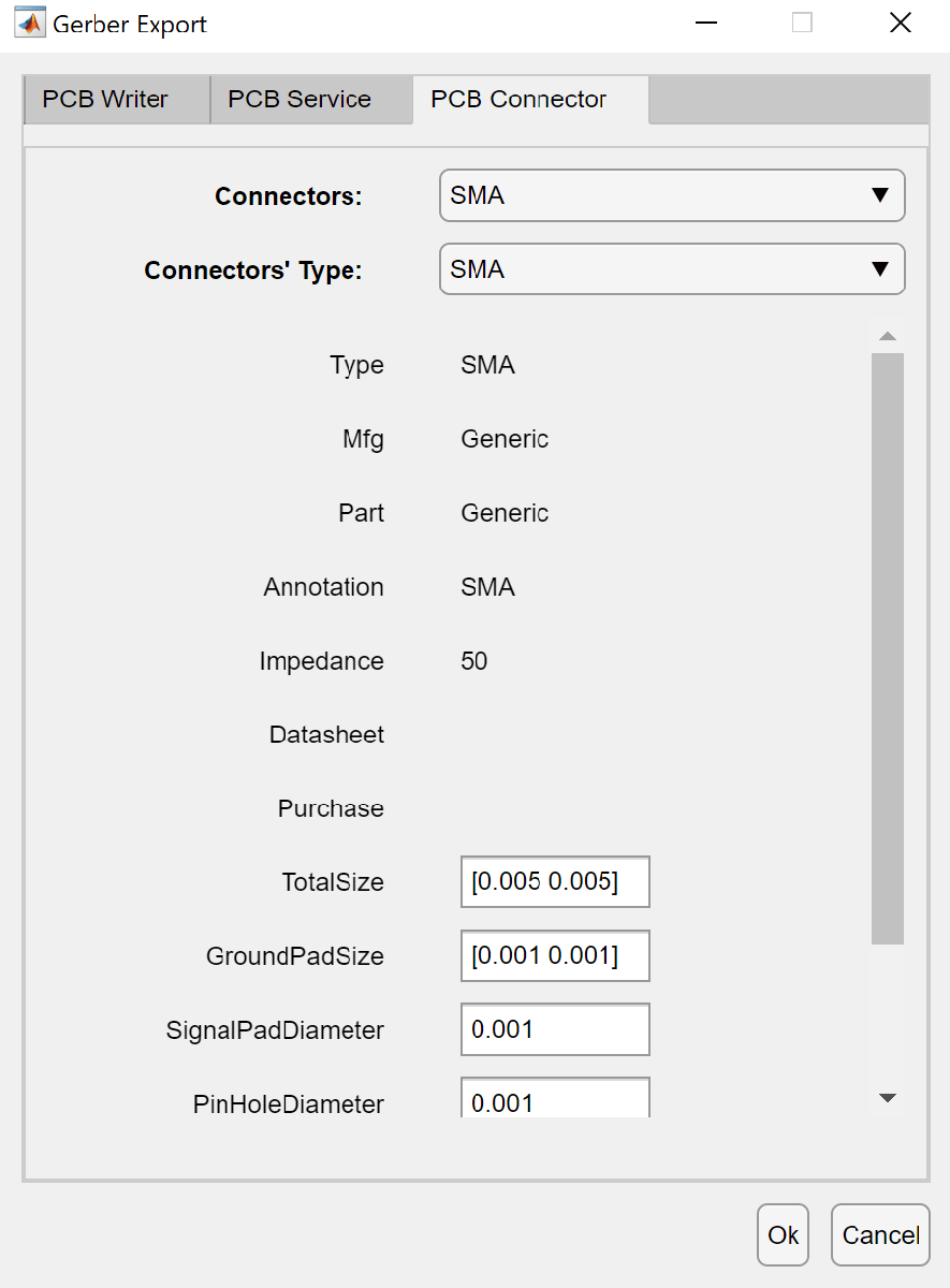
In the PCB Connector tab, set Connectors and Connectors' Type to SMA.
Select OK to generate the Gerber files. The generated Gerber files are stored in the directory you selected in the PCB Writer tab.
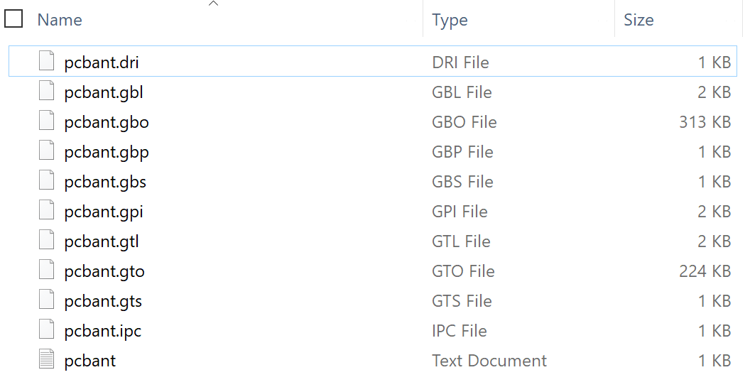
Open mayhewlabs web Gerber interface (https://mayhewlabs.com/webGerber/) from your browser. Drag and drop the Gerber files from the directory and select Done.

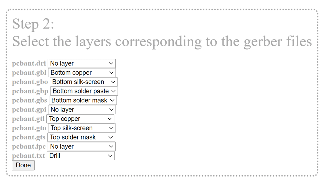
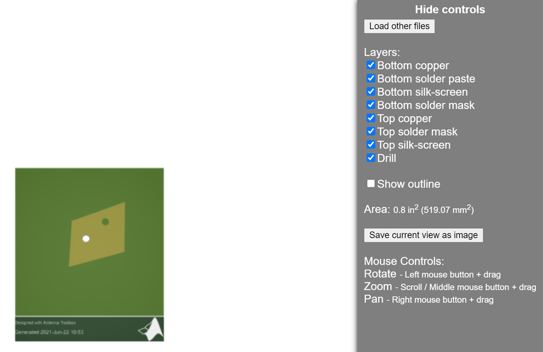
The Gerber files are displayed in the Gerber viewer. You can use the Gerber files in the fabrication of your PCB patch antennas.
You can also export your design to the MATLAB workspace or MATLAB script by selecting Export to MATLAB Workspace or Export to MATLAB Script under the Export in the Design or Analysis tab.
Related Examples
Programmatic Use
Version History
Introduced in R2021b