Design and Analysis Using PCB Antenna Designer
This five part tutorial shows how to design, validate, analyze, optimize and export a 1-by-2 linear array of H-notch patch antennas resonating at 4.65 GHz using the PCB Antenna Designer app. The first four parts of this tutorial are sequenced as: define the PCB layers, design and analyze the unit element, create a linear array, and export the design. The fifth part of this tutorial allows you to recreate the same H-notch patch using variables for property values and optimize the design for maximum gain.
To get started, follow these steps:
Define PCB Antenna layers: Define the metal patch, substrate, and ground plane layers for the linear array of 1-by-2 H-notch patch PCB antenna. For more information, see Define PCB Antenna Layers.
Design H-notch patch unit element: Design the H-notch patch unit element by subtracting the top and bottom notches from the substrate. Add a feed to the H-notch patch unit element and validate the board shape, layers, feed, via, and load. For more information, see Design H-Notch Patch Unit Element.
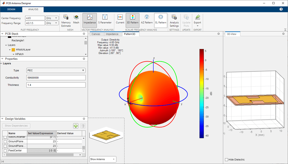
Analyze H-notch patch unit element: Perform vector frequency analysis on the H-notch patch unit element to calculate the impedance and the S-parameters over its frequency range of operation. Perform scalar frequency analysis on the H-notch patch unit element to calculate its current distribution, 3-D pattern, and azimuth and elevation patterns. For more information, see Analyze H-Notch Unit Element.
Create, analyze, and export 1-by-2 linear array of H-notch patch: Create a 1-by-2 linear array with the H-notch patch as unit element. Add the feed and validate the design before analysis. Analyze the design to confirm that it meets the design goals and export the design to Gerber files for the fabrication of the PCB patch antenna. For more information, see Design, Analyze, and Export 1-by-2 H-Notch Linear Array.
Design, analyze, and optimize H-notch patch using design variables: Design the same H-notch patch using variables for the properties of the board, metal layers, and patch. Create these variables using the Design Variables tab. Analyze the design to see that the results match the pervious patch. Optimize the design for maximum gain. For more information see, Design, Analyze, and Optimize H-Notch Patch Using Design Variables.