主要内容

Design, Analyze, and Export 1-by-2 H-Notch Linear Array

R2026b

This step of the tutorial shows how to design, analyze, and export a 1-by-2 H-notch linear array.

Design 1-by-2 H-Notch Linear Antenna Array

Select HNotchLayer in the PCB Stack pane and drag the axes to create a selection box. Drag the axes until the selection box encloses Feed and HNotchLayer.
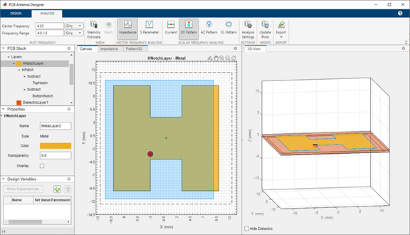
PCB Antenna Designer app canvas showing a 2D top view and a 3D view of an H‑shaped PCB antenna layout, with layer settings and properties displayed in a left panel.

Click Copy on the Design tab to copy the layers enclosed in the selection box and click Paste to create the HPatch_Copy(1) layer.
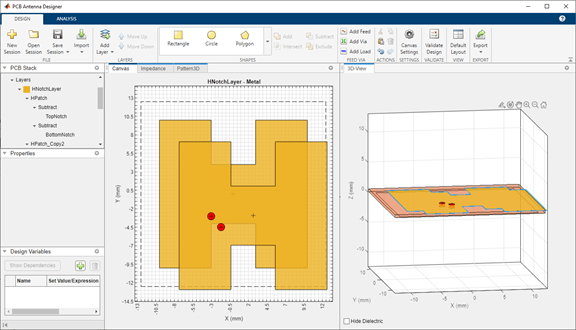
PCB Antenna Designer app canvas showing a 2D top view and a 3D view of an H‑shaped copper patch with feed markers. The left panel lists PCB layers and properties, the center panel displays the 2D layout, and the right panel shows the 3D stackup view.

Select the HPatch_Copy(1) layer and drag it to place it to adjacent to the HPatch layer.
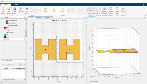
A screenshot of the PCB Antenna Designer app canvas. A toolbar at the top contains options for adding shapes, feeds, vias, and analyzing the design. The left panel lists PCB stack layers and design variables. The main canvas shows a 2D top‑view of two H‑shaped antenna patches with feed points marked by red dots. To the right, a 3D visualization displays the antenna structure on a substrate within an axis‑labeled grid.

Validate Design for Errors

Click Validate Design on the toolbar to validate your board shape, layers, feed, via, and load. The Check Layers and Check Feed validation failed because HNotchLayer and Feed1_Copy(1) lie outside BoardShape and GroundPlane, respectively.
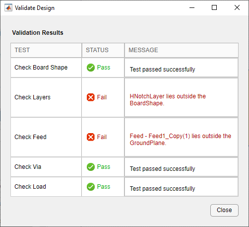
A dialog box for design validation showing validation results.

Overlay Layers

Select HNotchLayer and then select the Overlay check box in the Properties pane to create an image of HNotchLayer in the canvas.
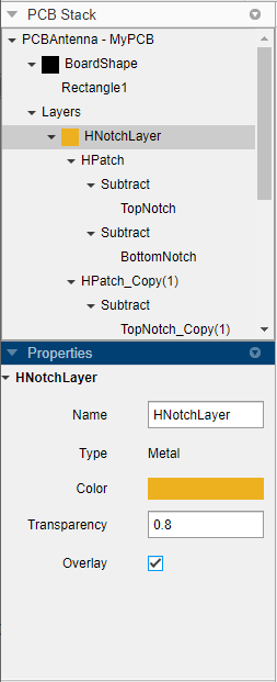
PCB Antenna Designer property panel showing “HNotchLayer” layer selected in the PCB Stack panel. The Properties panel displays the layer’s settings: Name “HNotchLayer,” Type “Metal,” yellow color, Transparency 0.8, and Overlay enabled.

Select Rectangle1 under BoardShape on the canvas and use the marker on the right to change the shape of BoardShape such that it encloses the HNotch image.
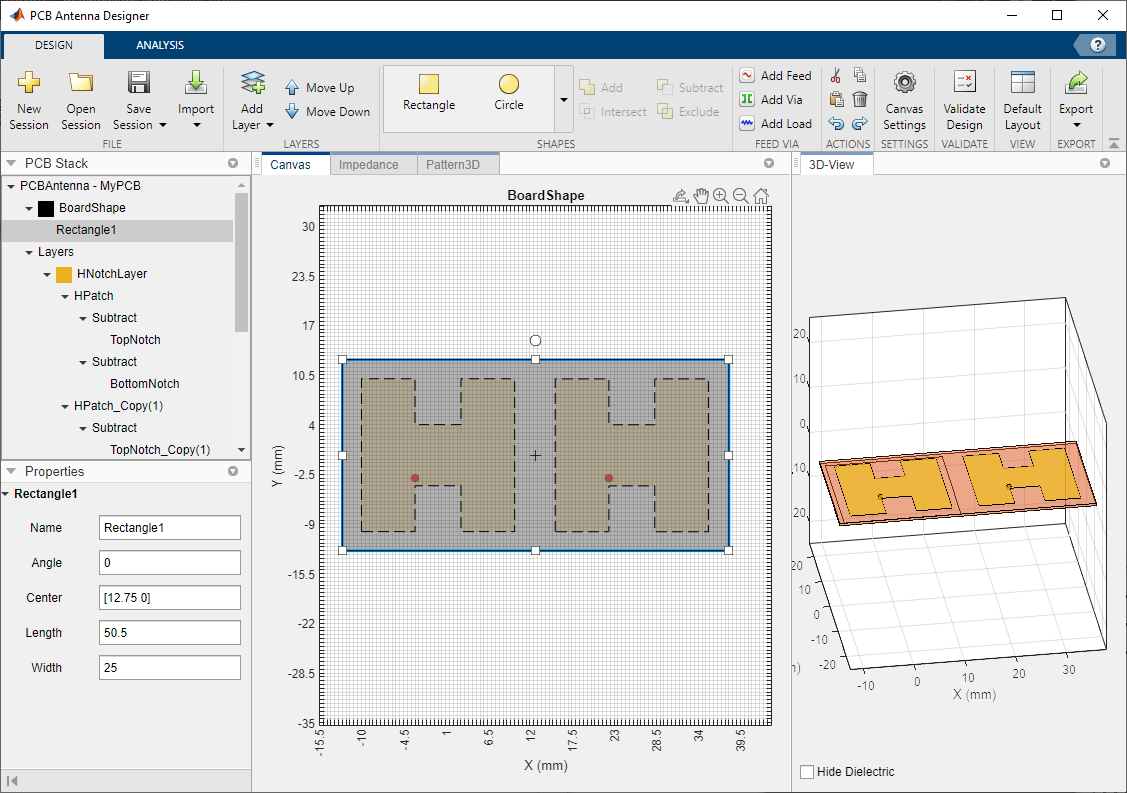
Screenshot of PCB Antenna Designer canvas showing a workspace with a dual‑section H‑shaped antenna layout. The central canvas displays a rectangular board outline with two mirrored H‑shaped copper patterns inside it, each marked with a red point near the center. On the right side, a 3D view panel shows the same antenna geometry rendered in perspective. The left sidebar lists layers and shapes, while the top toolbar includes options for editing, shapes, layers, feed insertion, and exporting.

Repeat the procedure with the GroundPlane layer.
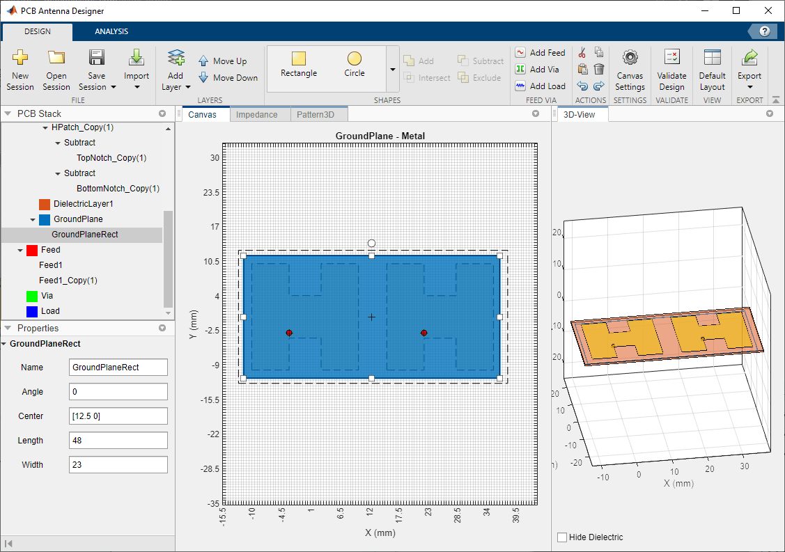
Screenshot of the PCB Antenna Designer app canvas. The left pane shows a hierarchical list of PCB stack elements, including layers such as ‘DielectricLayer1’, ‘GroundPlane’, and objects like feeds and vias. The center pane displays a top‑down 2D view of a rectangular blue ground plane labeled ‘GroundPlane – Metal,’ with grid lines, axis labels, and movable corner handles. Two red markers appear inside the rectangle. The right pane shows a 3D rendered view of the PCB design with copper structures on a tilted board. Toolbars at the top contain options for shapes, layers, feeds, loads, simulation, and export.

The BoardShape now encloses the HNotchLayer. You can change the layer dimensions using the Properties pane.

Validate Design for Errors

Click Validate Design to check for issues in the design. The design is validated with no errors.
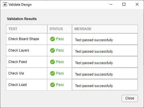
A dialog box for design validation showing validation results.

Run Analysis

Click Update Plots in the Analysis tab to update the analysis results. This updates all the analysis plots in the app for the design of a 1-by-2 H-notch linear array.

3-D Pattern

The pattern for the antenna is more directional with a higher gain compared to the H-notch patch unit element. The directivity of the 1-by-2 H-notch linear array is 7.66 dBi.
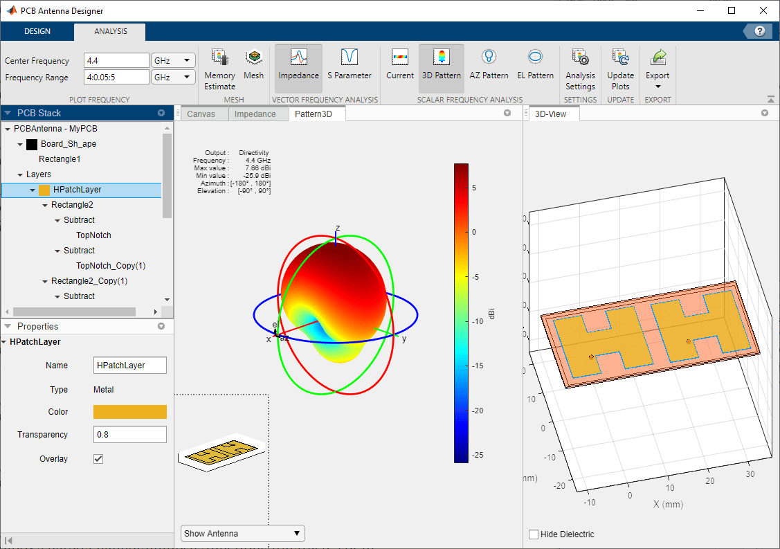
A screenshot of the PCB Antenna Designer app canvas. The window shows a PCB stack design on the left panel with layers listed, including rectangles, substrates, and patches. The center panel displays a 3D radiation pattern plot with colored lobes and a vertical color scale ranging from –25 to +5. The right panel shows a tilted 3D view of a PCB layout featuring two H‑shaped copper patches on a substrate grid. Various toolbars and tabs such as Design, Analysis, Mesh, Impedance, S Parameter, 3D Pattern, and export options are visible across the top.

Export Your Design to Gerber Files

In the Analysis tab, click Export and then select Export as Gerber File. In the Gerber Export dialog box, select Browse in the PCB Writer tab to select the directory in which you want the Gerber files to be stored.
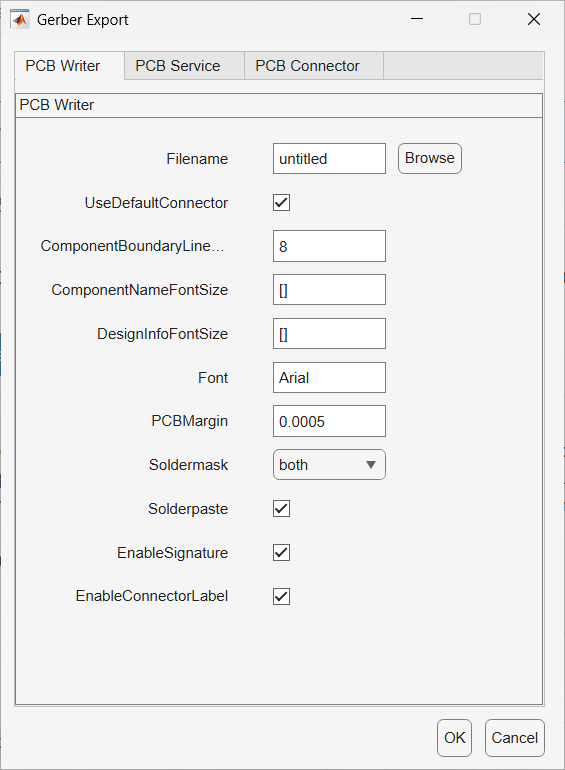
A screenshot of the “Gerber Export” settings window with four tabs at the top: “PCB Writer,” “PCB Service,” “PCB Connector,” and again “PCB Writer,” which is selected. The panel displays various export options including a filename field set to “untitled” with a “Browse” button. Several checkboxes appear, including “UseDefaultConnector,” “Solderpaste,” “EnableSignature,” and “EnableConnectorLabel,” all checked. Text fields include values such as “8” for ComponentBoundaryLine, empty brackets for ComponentNameFontSize and DesignInfoFontSize, “Arial” for Font, and “0.0005” for PCBMargin. A dropdown menu labeled “Soldermask” is set to “both.” At the bottom, there are “OK” and “Cancel” buttons.

Clear the UseDefaultConnector check box.
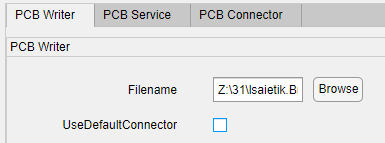
A cropped screenshot of the “PCB Writer” settings panel. The top shows three tabs: “PCB Writer,” “PCB Service,” and “PCB Connector,” with “PCB Writer” selected. Below, there is a “Filename” field containing the path and a “Browse” button. A checkbox labeled “UseDefaultConnector” appears underneath and is unchecked.

In the PCB Services tab, under Services, select GerbLookWriter. The PCB writer uses the selected service to create the Gerber files.
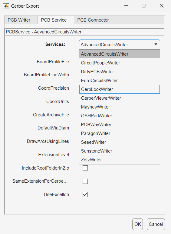
PCB writer service selection menu. The GerbLookWriter is selected.

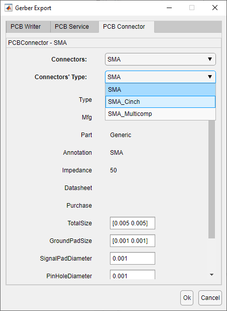
In the PCB Connector tab, set Connectors to SMA and Connectors' Type to SMA_Cinch.
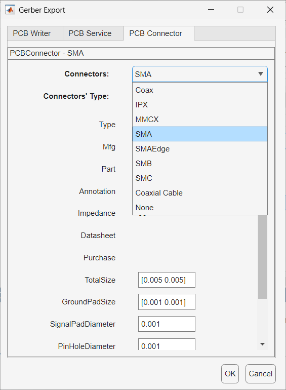
PCB Connector selection menu. SmaCinchDropdown.PNG

The PinHoleDiameter is of the same value as the FeedDiameter. Click OK to generate the Gerber files.
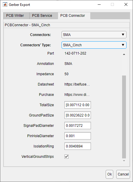
SmaCinchPinHolediameter.PNG

The generated Gerber files are stored as a .zip file in the directory that you selected in the PCB Writer tab.
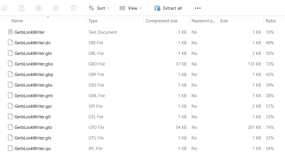
Folder containing Gerber files.

Open gerblook web Gerber interface from your browser. Click to upload, or drag and drop the zip-file from the directory.
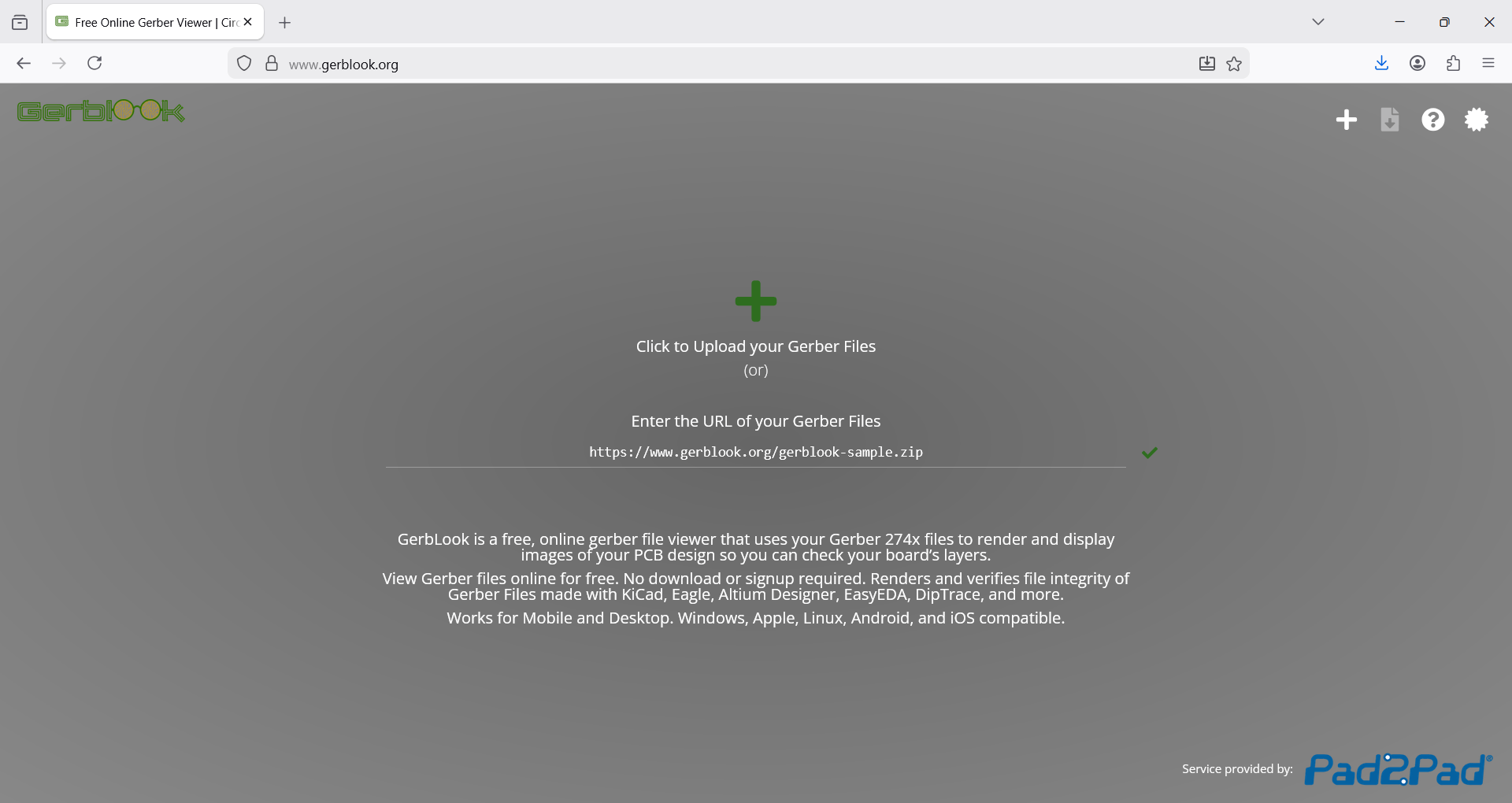
Online gerblook gerber viewer.

The Gerber files are displayed in the Gerber viewer. You can use the Gerber files to fabricate your 1-by-2 H-notch linear array.

All the layers overlayed:
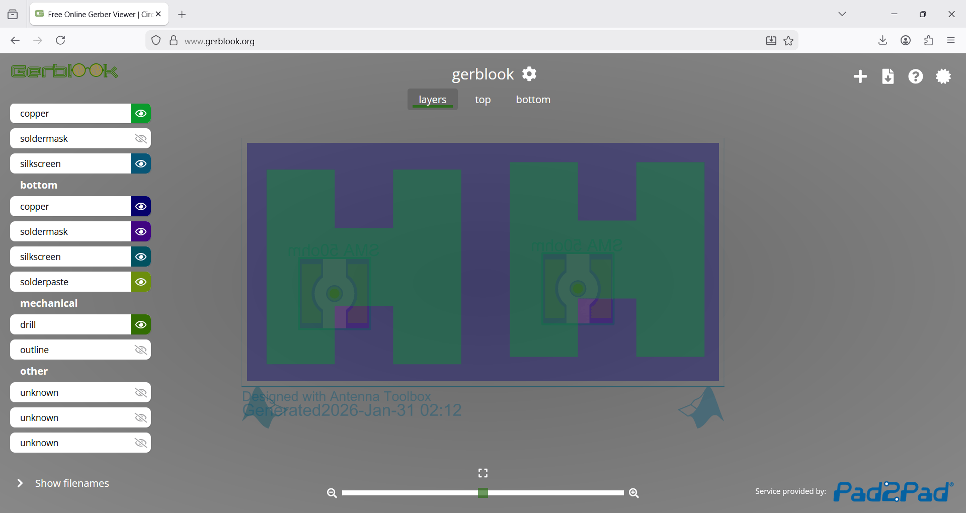
All the layers of the PCB as viewed in the online gerber viewer.

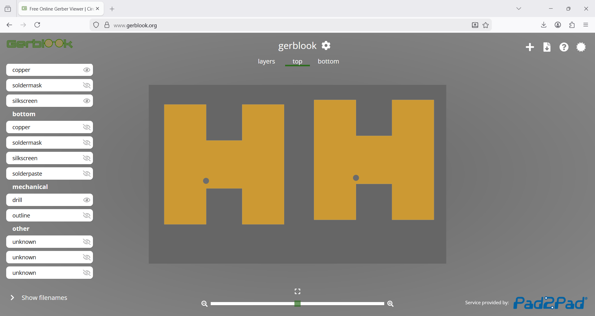
Top Layer:

Top layer of the PCB.

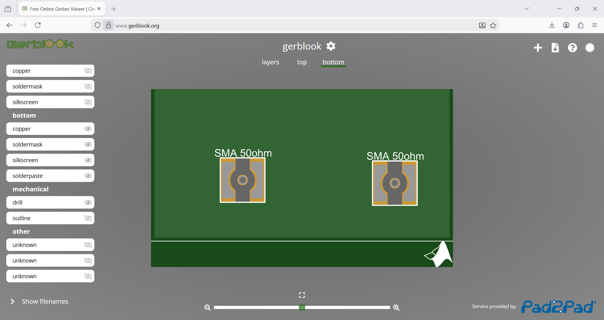
Bottom Layer:

Bottom layer of the PCB.

You can also export your design to the MATLAB® workspace or MATLAB script by selecting Export to MATLAB Workspace or Export to MATLAB Script under Export in the Design or Analysis tab.

See Also

Objects

Functions