Algorithm Verification with a FIL Source Block
This example shows how to verify an HDL design quickly and efficiently using FPGA-in-the-Loop (FIL). The testbench is synthesized together with the Design Under Test (DUT), the result is downloaded to an FPGA board, and the test is run with FIL. Using FIL for this process enables high speed generation and processing of test stimulus, with results returned to Simulink® for analysis. This example executes these tasks for an image processing use case.
Requirements
Tools required for this example:
Signal Processing Toolbox™
FPGA design software
One of the supported FPGA development boards and accessories (the ML403 board is not supported for this example). For more information about supported hardware, see Supported FPGA Devices for FPGA Verification.
For connection using Ethernet: Gigabit Ethernet Adapter installed on host computer, Gigabit Ethernet crossover cable
For connection using JTAG: USB Blaster I or II cable and driver for Intel FPGA boards. Digilent® JTAG cable and driver for AMD® FPGA boards.
For connection using PCI Express®: FPGA board installed into PCI Express slot of host computer.
Sobel Edge Detection

The sobel_edge_hardware subsystem is the algorithm to be synthesized into an FPGA. The stimulus is a gif file containing the image (a stop sign). In this example the image is moved inside the FPGA along with the algorithm, a FIL block is created for that FPGA design.
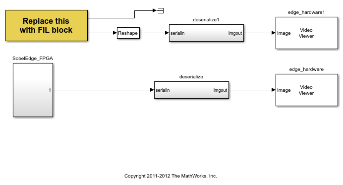
The steps taken to implement this technique are illustrated in the model fil_sobel_model. In this model, the gif file is contained by a lookup table and a counter is used to scan through the lines in the image and send them to the algorithm. The FIL block is added to the model in parallel with the behavioral blocks to enable directly checking the outputs of the FPGA against the behavioral model as a simple example of results analysis. Click the button to open the model.
Generate HDL Code
If you have HDL Coder™, you can generate code for the "SobelEdge_FPGA" subsystem using the HDL Workflow Adviser or Configuration Parameter UI (see HDL Coder documentation for more information).
If you do not have HDL Coder, you can use the pre-generated HDL files in the current directory.
Set Up FPGA Design Software
Before using FPGA-in-the-Loop, make sure your system environment is set up properly for accessing FPGA design software. You can use the function hdlsetuptoolpath to add FPGA design software to the system path for the current MATLAB® session.
Configure and Build FPGA-in-the-Loop
The FIL Wizard guides you in configuring settings necessary for building FPGA-in-the-Loop. Launch the wizard with the following command:
filWizard;
1. In Hardware Options, select the FPGA development board connected to your host computer. If necessary, you can also customize the Board IP and MAC Address under Advanced Options. Click Next to continue.
2. In Source Files, add the following generated HDL files for the design to the source file table using Browse.
SobelEdge_FPGA.vhd,
DualPortRAM_128x9b.vhd
DualPortRAM_128x9b_block.vhd
sobel_edge_eml.vhd
sobel_edge_hardware.vhd
SobelEdge_FPGA_pkg.vhd
u_d_ram.vhd
u_d_ram_block.vhd
Check the top-level checkbox next to SobelEdge_FPGA. Click Next to continue.
3. In DUT I/O Ports, the input and output port information, such as port name, direction, width and port type are automatically generated from the HDL file. Port types, such as Clock and Data, are generated based on port names; you may change the selection as necessary. For this example, the generated port types are correct, and you can click Next.
4. In Build Options, specify the folder for FIL output files. You can use the default value for this example. Click Build. Clicking Build causes the FIL Wizard to generate all the necessary files for FPGA-in-the-Loop simulation and perform the following actions:
Generates a FIL block in a new Simulink model
Opens a command-line window to compile the FPGA project and generate the FPGA programming file
The FPGA project compilation process takes several minutes. When the process is finished, you are prompted to close the command-line window. Close this window now.
Configure FIL Block
To prepare for FPGA-in-the-Loop simulation, follow the steps below to configure the FIL block.
1. Open the testbench model fil_sobel_model and copy the generated FIL block into the model.
2. Double-click the FIL block to open the block mask. Click Load to program the FPGA with the generated programming file.
3. Under Runtime Options, change Overclocking factor to 1. This specifies that each input value is sampled once by the FPGA clock before the input changes value.
4. Set the output frame size to 20000.
5. On the FIL block mask, click on the Signal Attributes tab. Change the data type for out1 to boolean to match the data type of the behavioral Sobel block.
5. Click OK to close the block mask.
Results
The model provided in this example will compare the results obtained from the behavioral block with those from the FPGA. You can run that model and observe the equivalence. You can also observe the relative simulation performance of the behavioral simulation and the FIL simulation by creating a new model containing only the behavioral path and another containing only the path with the FIL block. Run each of those models separately using:
tic;
sim(your_model_name);
toc
You can see that FIL is faster. This increase in speed is because there is only one FIL function call for 20000 samples while the behavioral model needs 20000 function calls to process all of the data. Therefore you will get better performance if the size of the image is bigger. This step concludes this example.