Create IBIS Model from Electrical Specifications
R2026bThis example shows how to use the IBIS Designer app to create a complete IBIS (I/O Buffer Information Specification) model from a set of electrical parameters derived from a datasheet or design specification. This workflow, called the Parameterized Model flow, generates IV curves, VT waveforms, and C_comp analytically without requiring SPICE simulation data.
Use this workflow to:
Explore early-stage designs before silicon characterization is available
Create representative models from datasheet specifications (driver impedance, rise/fall time, capacitance)
Quickly generate IBIS models for signal integrity simulation when SPICE netlists are not available
Setup
Open the IBIS Designer application by calling ibisDesigner at the MATLAB command line.
ibisDesigner
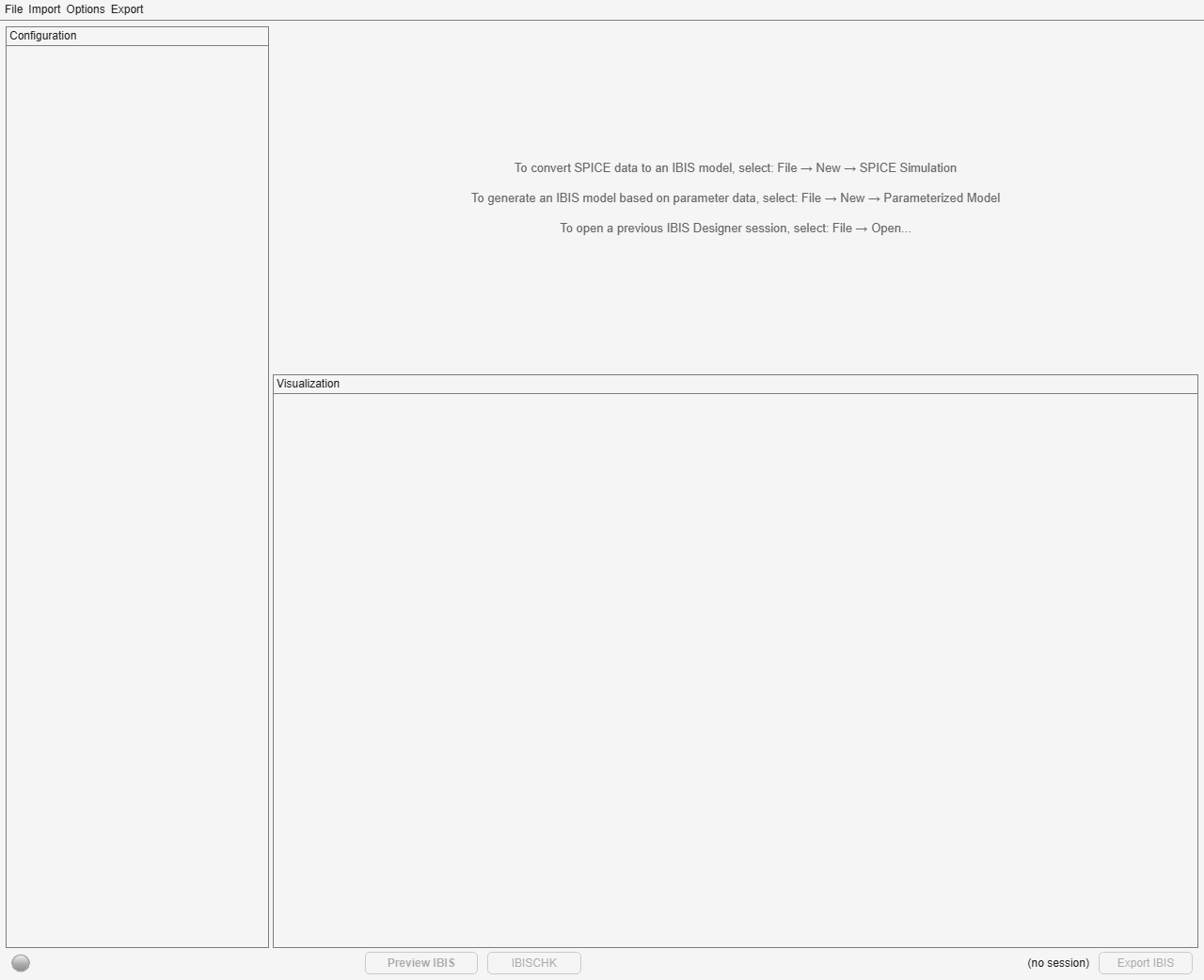
Create a Parameterized Model Session
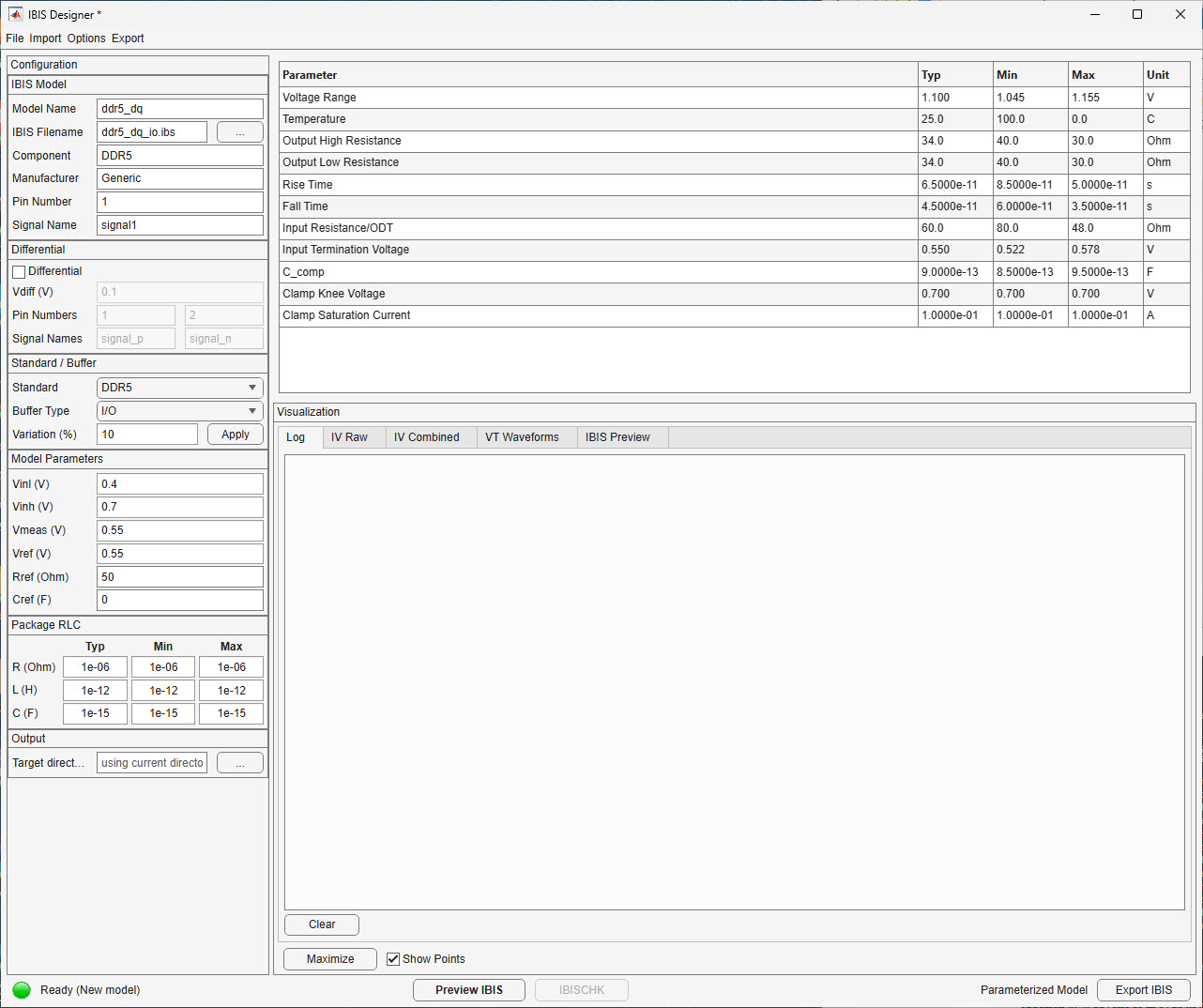
Select File > New > Parameterized Model from the menu bar. The main content area now shows the electrical parameters table, and the left panel displays the Configuration panel organized into sections: IBIS Model (model name, IBIS filename, component, manufacturer, pin number, signal name), Output (target directory for exported files), Standard / Buffer (technology preset and buffer type dropdowns, variation percentage), Differential (enable differential mode, Vdiff, pin/signal pairs), and Package RLC (package resistance, inductance, capacitance).
Select a Technology Standard
The Standard / Buffer section of the Configuration panel contains two key dropdowns that control what kind of model is generated: Standard and Buffer Type.
The Standard dropdown provides technology presets that populate all electrical parameters with representative values for a given interface standard. Each preset is configured to a specific technology (DDR5, PCIe5, PCIe6, etc.) and sets appropriate supply voltage, driver impedance, edge rates, capacitance, and differential mode. Selecting a preset gives you a reasonable starting point; you can customize individual parameters afterward. In addition, there is a Custom Standard which does not contain any default values.
For this example, select DDR5 from the Standard dropdown. The parameters table populates with values representative of a DDR5 data buffer.
The Buffer Type dropdown determines which combination of IV curves and VT waveforms the model will contain to support various model types. The available types are:
Output: Generates only driver curves (Pulldown/Pullup IV, VT waveforms, Ramp). Use for models that only transmit.
Input: Generates only receiver curves (GND Clamp and Power Clamp IV from on-die termination). Use for models that only receive.
I/O: Generates both driver and receiver curves. This is the most complete model type, suitable for bidirectional models.
3-state: Generates driver curves plus a high-impedance state. Use for models that can tri-state.
Set the Buffer Type to I/O. This is the appropriate choice for a DDR5 DQ model, which operates in both transmit and receive modes during read and write bursts.
Review and Customize Electrical Parameters
The main content area displays the electrical parameters table. This table has five columns: Parameter, Typ, Min, Max, and Unit. The Parameter column shows the name of each electrical quantity, the Typ, Min, and Max columns hold the numerical values for the three IBIS process corners, and the Unit column shows the engineering unit for each row. After selecting the DDR5 preset and I/O buffer type, all rows are populated with representative values for that standard.
For an I/O buffer, the parameters table contains the following eleven required entries:
Voltage Range
The Voltage Range parameter sets the supply voltage (Vdd) of the I/O buffer. This single value defines the rail-to-rail voltage swing of the output driver: the Pulldown IV curve sweeps from 0 V to the Voltage Range value, and the Pullup IV curve is referenced to this same rail. It also defines the boundary between the Power Clamp and GND Clamp regions: the GND Clamp is active below 0 V, while the Power Clamp is active above the Voltage Range. In the generated IBIS file, this value appears as the voltage_range keyword under the [Model] section and sets the Vcc reference level for all IV and VT data tables. If your design uses a 1.1 V supply (typical for DDR5), the Typ column should read 1.1.
Temperature
The Temperature parameter sets the junction temperature of the die for each process corner. Temperature affects the electrical behavior of the buffer through carrier mobility and threshold voltage variations, though in the Parameterized Model workflow, temperature is recorded as metadata in the IBIS file rather than used to modify the curves directly. The IBIS specification requires temperature values in the [Temperature Range] keyword: a typical value (usually 25 °C for room temperature), a minimum value (the hot corner, typically 100 °C, representing weakest drive strength), and a maximum value (the cold corner, typically 0 °C or -40 °C, representing strongest drive strength). Note that in IBIS terminology, "min" refers to minimum drive strength (hot), not minimum temperature.
Output High Resistance
The Output High Resistance parameter specifies the equivalent pull-up resistance (in ohms) of the output driver when driving a logic-high level. This resistance represents the combined on-resistance of the PMOS pull-up network in the output stage. It directly controls the slope of the Pullup IV curve: a lower resistance produces a steeper curve (stronger drive), while a higher resistance produces a shallower curve (weaker drive). In the generated IBIS model, this value shapes the Pullup IV table; the current at each voltage point equals the voltage difference from the supply rail divided by this resistance. For DDR5, where the output impedance is typically matched to the transmission line characteristic impedance, this value is set near the target impedance of the channel (e.g., 34 ohms for a 34-ohm output impedance specification).
Output Low Resistance
The Output Low Resistance parameter specifies the equivalent pull-down resistance (in ohms) of the output driver when driving a logic-low level. This resistance represents the combined on-resistance of the NMOS pull-down network in the output stage. It directly controls the slope of the Pulldown IV curve: lower resistance means the driver can sink more current at a given voltage, resulting in a stronger low-side drive. The Pulldown IV curve current at each voltage point equals the pad voltage divided by this resistance. For symmetric driver designs (equal pull-up and pull-down strength), Output Low Resistance is set equal to Output High Resistance. For designs with asymmetric drive strength (common in some older standards), these two values differ.
Rise Time
The Rise Time parameter specifies the 20%-to-80% transition time (in seconds) for a rising edge at the output. This is the time it takes for the output voltage to transition from 20% of the supply voltage to 80% of the supply voltage when the driver switches from low to high. IBIS Designer uses this value to generate the rising VT (voltage-vs-time) waveforms by constructing an RC-shaped transition whose time constant produces the specified 20%-80% crossing time. The VT waveforms are simulated into standard 50-ohm fixture loads terminated to both GND and Vdd. In the generated IBIS file, this value also determines the rising Ramp rate (dV/dt) reported in the [Ramp] section. Typical DDR5 rise times are in the tens of picoseconds (e.g., 65 ps), reflecting the high-speed edge rates required by the standard.
Fall Time
The Fall Time parameter specifies the 80%-to-20% transition time (in seconds) for a falling edge at the output. This is the time it takes for the output voltage to transition from 80% of the supply voltage to 20% of the supply voltage when the driver switches from high to low. Like Rise Time, this value shapes the falling VT waveforms and determines the falling Ramp rate (dV/dt). In many designs, the Fall Time is shorter than the Rise Time because NMOS transistors (which drive the falling edge) typically have higher mobility than PMOS transistors (which drive the rising edge). The VT waveform generation uses the same RC-shaping approach as the rising edge, but applied to the high-to-low transition.
Input Resistance/ODT
The Input Resistance/ODT parameter specifies the on-die termination (ODT) resistance (in ohms) that is active when the buffer operates in receive mode. On-die termination absorbs signal reflections at the receiver pad by providing an impedance-matched termination on the die itself, eliminating the need for external termination resistors. In the Parameterized Model, this resistance is split into two legs using a Thevenin-equivalent network centered on the Input Termination Voltage: one leg from the pad to Vdd and one leg from the pad to ground. The split generates the GND Clamp and Power Clamp IV curves that represent the receiver input behavior. For DDR5, ODT values are programmable and typically range from 34 to 240 ohms depending on the selected termination strength register setting.
Input Termination Voltage
The Input Termination Voltage parameter specifies the DC bias voltage (in volts) of the on-die termination network. This is the voltage at which the receiver pad settles when no signal is being driven (the quiescent termination point). The Thevenin-split of the ODT resistance is computed so that the open-circuit voltage equals this value. For a standard DDR5 configuration, the Input Termination Voltage is set to Vdd/2 (0.55 V for a 1.1 V supply), placing the termination midpoint at the center of the signal swing for optimal noise margins in both high and low states. This value directly affects the shape and DC offset of the GND Clamp and Power Clamp IV curves generated for the receiver.
C_comp
The C_comp parameter specifies the total die capacitance (in farads) seen at the pad of the I/O buffer. This capacitance includes contributions from the ESD protection structures, the output driver transistor gate/drain capacitances, the input receiver gate capacitance, metal routing parasitics on the die, and any intentional decoupling. In the generated IBIS file, this appears as the C_comp value in the [Model] section. Signal integrity simulators use C_comp as a lumped capacitive load at the buffer pad to model the capacitive loading effect of the die on the transmission line. Typical DDR5 C_comp values are in the sub-picofarad range (e.g., 0.5 to 1.5 pF). Accurate C_comp values are important for predicting signal attenuation, impedance discontinuities, and timing at the receiver.
Clamp Knee Voltage
The Clamp Knee Voltage parameter specifies the voltage offset (in volts) beyond the supply rails at which the ESD protection clamp diodes begin to conduct significant current. The GND Clamp diode turns on when the pad voltage drops below -(Clamp Knee Voltage), and the Power Clamp diode turns on when the pad voltage rises above Vdd + (Clamp Knee Voltage). A smaller knee voltage means the clamps activate closer to the rails, providing tighter voltage clamping but potentially interfering with normal signal swings that overshoot. A larger knee voltage means the clamps remain inactive until larger overshoots occur. In the generated IV curves, this parameter controls the "elbow" point where the clamp characteristic transitions from near-zero current to exponentially rising current.
Clamp Saturation Current
The Clamp Saturation Current parameter specifies the maximum current (in amperes) that the ESD protection clamp diodes can conduct when fully activated. In the clamp model, an exponential diode equation generates the IV curve shape near the knee, but the current is hard-limited to the Clamp Saturation Current value. This ceiling caps how much current the clamp can sink or source regardless of how far the voltage exceeds the rails. A larger value allows the clamp to conduct more current during large overshoots (stronger protection), while a smaller value limits the clamp's ability to absorb energy. Typical values are in the range of tens to hundreds of milliamps (e.g., 100 mA for DDR5), representing the current capacity of the on-die ESD protection structures. This parameter primarily affects the flat portion of the clamp IV curves beyond the knee: once the voltage exceeds the Clamp Knee Voltage threshold, the current rises exponentially until it saturates at this value.
You can edit any value directly in the table by clicking its cell. For this example, leave the DDR5 defaults as-is.
Apply Corner Variation
IBIS models require data for three process corners: typical (typ), minimum (min/slow), and maximum (max/fast). Rather than manually computing each corner value, IBIS Designer can automatically derive min and max values from the typical values using a percentage variation.
The Variation (%) field is located in the Standard / Buffer section of the Configuration panel. Enter 8 and click Apply. This populates all Min and Max columns using the IBIS corner convention:
Min corner (slow): Higher resistance (+%), lower voltage (-%), longer transition times (+%), higher capacitance (+%), higher temperature. This represents worst-case drive strength.
Max corner (fast): Lower resistance (-%), higher voltage (+%), shorter transition times (-%), lower capacitance (-%), lower temperature. This represents maximum drive strength.
The sign of the variation is determined by the parameter's physical role: parameters that weaken the driver when they increase (resistance, edge time) get a positive offset for the slow corner, while parameters that strengthen the driver when they increase (voltage) get a negative offset for the slow corner. Capacitance follows a different convention: a slow (heavily loaded) buffer has higher C_comp, so the slow corner gets the positive offset.
Note on IBIS C_comp ordering: The IBIS specification requires that C_comp values appear in numeric order (typ/min/max), where "min" and "max" refer to the numeric value, not the corner name. Because a slow buffer has higher capacitance, the numerically maximum C_comp value corresponds to the Min (slow) corner, and the numerically minimum C_comp value corresponds to the Max (fast) corner. IBIS Designer handles this mapping automatically; you only need to verify that the slow corner shows the larger capacitance value.
After applying, inspect the Min and Max columns to verify the values look reasonable.
Configure Model Identity
The IBIS Model section of the Configuration panel contains fields that define how this model appears in the generated IBIS file. Set the following values:
Model Name:
ddr5_dq_io. This becomes the[Model]keyword in the IBIS file. Must be unique within the file. EDA tools reference this name when assigning models to pins.Component:
DDR5_PHY. This becomes the[Component]keyword, typically representing the chip or die that contains this buffer.Manufacturer:
Generic. Identifies the silicon vendor in the IBIS file header.Pin Number:
A1. The pin identifier that appears in the[Pin]table.Signal Name:
DQ0. The signal name associated with this pin. Defaults to the Model Name if left blank.
These fields map directly to IBIS file keywords. When you later use this model in a signal integrity simulator, you reference it by the Model Name and associate it with physical pins via the Pin Number and Signal Name fields.
Differential Configuration
The Differential section provides an optional checkbox and fields for differential pin pairs. When the Differential checkbox is enabled, the generated IBIS file includes a two-pin [Pin] table and a [Diff Pin] section that pairs the non-inverting and inverting pins. The fields mirror those in the IBIS Model section:
Vdiff (V): The differential input voltage threshold written to the
[Diff Pin]table. Default is 0.1 V.Pin Numbers: Two fields specifying the pin identifiers for the positive and negative pins of the pair (e.g.,
A1andB1).Signal Names: Two fields specifying the signal names for each pin (e.g.,
DQ0_pandDQ0_n).
For this DDR5 single-ended DQ example, leave the Differential checkbox unchecked. Differential mode is used for signals like DQS (data strobe) or CK (clock) that are routed as complementary pairs.
Configure Package RLC
The Package RLC section of the Configuration panel specifies the lumped parasitic model for the package trace between the die pad and the external ball/pin. These values populate the [Package] keyword in the IBIS file, which signal integrity simulators use to model the package interconnect.
The section contains a 3x3 grid of numeric fields with column headers Typ, Min, and Max:
R (Ohm): Series resistance of the package trace. Default is 0.001 milliohms (effectively zero for a short wirebond or bump).
L (H): Series inductance. Default is 1e-12 H (1 pH). Typical wirebond packages have 1-5 nH; flip-chip packages are much lower.
C (F): Shunt capacitance. Default is 1e-15 F (1 fF). Represents the parasitic capacitance of the package pad and routing.
Each parameter accepts per-corner values (typ/min/max). For this example, the default near-zero values are acceptable because the emphasis is on the buffer model rather than the package. For production models, obtain package RLC values from your package vendor's datasheet or extraction tool.
The [Package] section appears in the generated IBIS file between the [Component] header and the [Pin] table. Simulators add this lumped RLC network in series between the die model and the board-level transmission line.
Generate IBIS Model
Click the Preview IBIS button in the action bar at the bottom of the window. This performs the following steps:
Collects all parameters from the Configuration panel
Generates Pulldown and Pullup IV curves using a linear resistive driver model bounded by the supply rails
Generates GND Clamp and Power Clamp IV curves using exponential diode models for ESD protection, plus Thevenin-split ODT termination curves
Generates rising and falling VT waveforms using RC-shaped transitions derived from the Rise Time and Fall Time parameters
Computes Ramp (dV/dt) from the 20%-80% transition of the VT waveforms
Sets C_comp directly from the C_comp parameter value
Assembles the complete IBIS model in memory
When all steps finish successfully, the status bar shows "Preview complete."
Review Results
After generation, the Visualization panel at the bottom of the window populates with results. Use the tabs to inspect each aspect of the generated model.
IV Curves
The IV Raw tab shows the generated IV curves. For an I/O buffer, six sub-tabs are available: Pulldown, Pullup, Pullup VR, Power Clamp, Power Clamp VR, and GND Clamp.
Pulldown: Current vs. pad voltage for the NMOS pull-down driver (ground-referenced). The slope is determined by Output Low Resistance.
Pullup: Current vs. pad voltage for the PMOS pull-up driver. The x-axis is converted from the Vcc-relative representation to absolute pad voltage (Vpad = Vcc - Vtable), making it easier to visualize where current flows relative to the supply rails.
Pullup VR: The same Pullup data plotted in its native voltage-relative (VR) form, exactly as it appears in the IBIS file. The x-axis is Vtable = Vcc - Vpad, so 0 V corresponds to the pad at Vcc. This is the format that IBIS simulators read directly.
Power Clamp: Current vs. pad voltage for the supply protection diode plus ODT pull-up leg. Like the Pullup tab, the x-axis is converted from Vcc-relative to absolute pad voltage for intuitive visualization.
Power Clamp VR: The same Power Clamp data in its native voltage-relative form as stored in the IBIS file. The x-axis is Vtable = Vcc - Vpad. This representation is what IBIS simulators use internally.
GND Clamp: Current vs. pad voltage for the substrate protection diode plus ODT pull-down leg. This curve is ground-referenced (x-axis is pad voltage directly), so no voltage-relative variant is needed.
Each curve shows typ (blue), min (green), and max (red) corners. The min corner shows weaker drive (lower current at the same voltage) due to higher resistance.
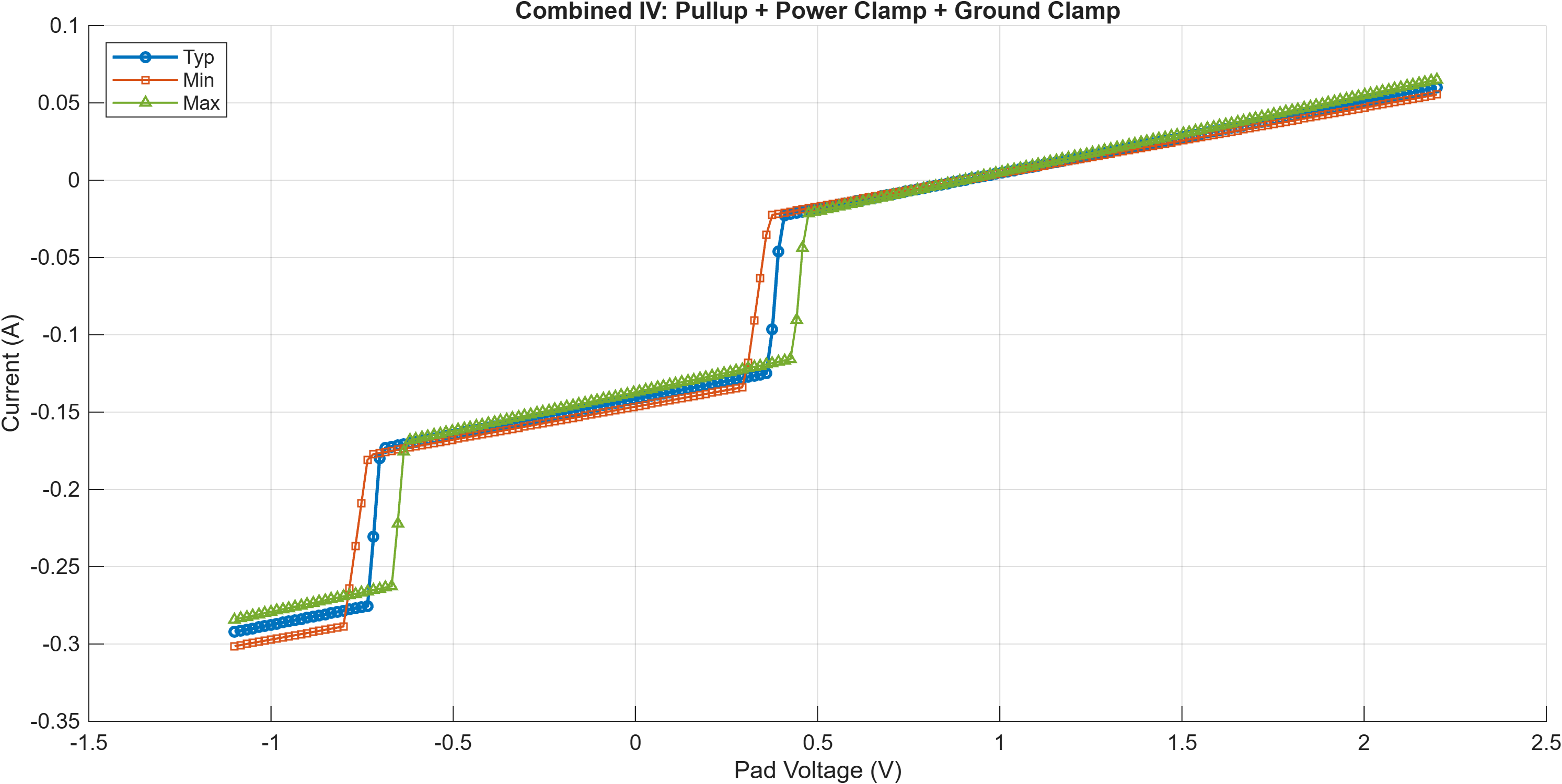
IV Combined
The IV Combined tab shows the total current that a signal integrity simulator would compute at the pad by summing the individual IV components. It has two sub-tabs:
Pulldown: Total output-low current: Pulldown IV + Power Clamp IV + GND Clamp IV, all interpolated to a common pad voltage grid from -Vcc to 2*Vcc.
Pullup: Total output-high current: Pullup IV + Power Clamp IV + GND Clamp IV, similarly interpolated to pad voltage.
These combined plots show what a receiver would see when the driver is in the low or high state. The clamp currents are negligible in the mid-range (between 0 and Vdd) but become significant near the rails, where the ESD clamp and ODT termination activate. Comparing the combined curves against the raw curves helps verify that the clamp and driver contributions interact correctly.
VT Waveforms
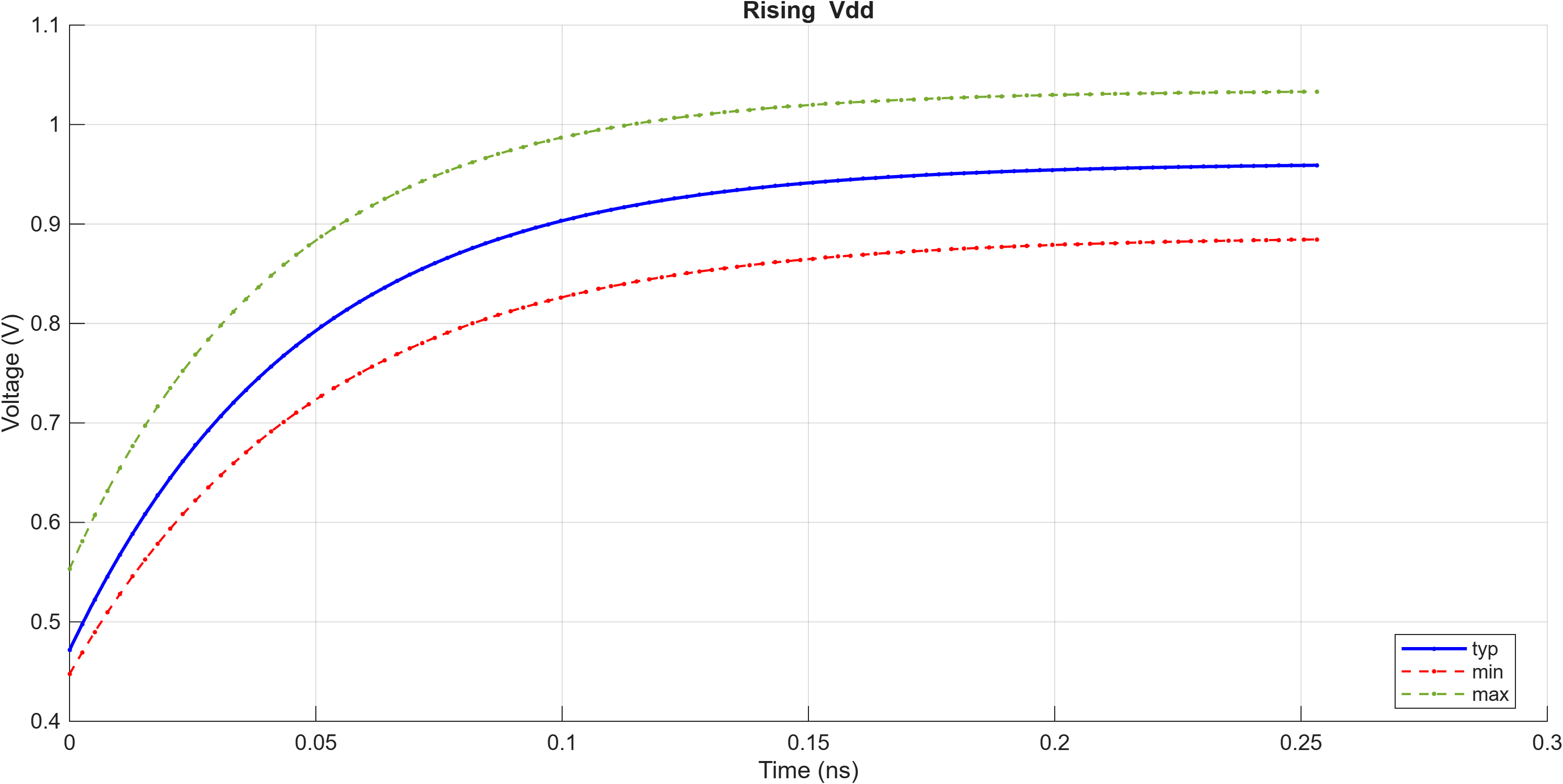
The VT Waveforms tab shows the transient voltage response at the buffer output when switching into a 50-ohm fixture load. Four waveforms are generated, each shown in a sub-tab:
Rising (GND): Output transitions from low to high into a load terminated to ground.
Rising (Vdd): Output transitions from low to high into a load terminated to Vdd.
Falling (GND): Output transitions from high to low into a load terminated to ground.
Falling (Vdd): Output transitions from high to low into a load terminated to Vdd.
The waveform shape follows an RC time constant derived from the Rise Time and Fall Time parameters and the driver-to-fixture impedance ratio. The typ corner shows the nominal transition, while the min corner (slow) shows a longer transition and the max corner (fast) shows a shorter transition.
IBIS Preview
The IBIS Preview tab shows the complete text of the generated IBIS file. Scroll through to verify the structure:
[IBIS Ver]header with version 6.1[Component]section with the configured component name and pin table[Model]section with Model_type I/O, C_comp values, and all IV/VT data tablesRamp data (dV/dt for rising and falling edges)
[End]keyword
Validate with IBISCHK (Optional)
Before exporting, you can validate the generated model against the IBIS specification by clicking the IBISCHK button in the action bar. This step is optional and requires a Signal Integrity Toolbox license.
The ibischk validator is the industry-standard compliance checker maintained by the IBIS Open Forum. It parses the generated IBIS file and checks for:
Errors: Specification violations that would prevent a simulator from reading the file correctly (e.g., non-monotonic IV data, missing required keywords, out-of-range values). These must be fixed before distributing the model.
Warnings: Informational notes about unusual values or absent optional fields (e.g.,
[Model Spec]not present, package parasitics near zero). Warnings are typically acceptable and do not affect simulator interoperability.
Results appear in the Logs tab of the Visualization panel and in the status bar, which shows a summary such as "Done. ibischk: 0 errors, 2 warnings". If errors are found, the status lamp turns amber and shows "Done with issues."
You can also enable automatic validation after every preview by selecting Options > Always Run IBISCHK from the menu bar. When enabled, IBIS Designer runs ibischk each time you click Preview IBIS, so you get immediate feedback as you iterate on parameters.
Export IBIS File
Click Export IBIS in the action bar to write the generated model to a .ibs file on disk. The file is saved to the Target directory specified in the Output section, using the filename from the IBIS Filename field in the IBIS Model section. If Target directory is blank, the current MATLAB working directory is used.
Save the Session
To preserve your work for later editing, save the session via File > Save (or File > Save As... to choose a new location). The session is stored as a .mat file (default name s2i_session.mat) that captures the complete app state:
All configuration panel settings (model identity, electrical parameters, corner values, variation percentage)
Loaded file paths (for SPICE Simulation sessions)
Conversion results and log output
Output directory and filename preferences
You can also use Export > Export to MATLAB to generate a standalone MATLAB script that recreates the current session programmatically. Unlike the session file (which stores internal app state), the exported script uses public API calls and is suitable for version control, automation, or batch processing.
Programmatic Equivalent
The entire workflow demonstrated above can be reproduced programmatically using the IBIS Designer public API. The following script generates the same DDR5 I/O model without opening the GUI:
params = struct();
Warning: Graphics acceleration hardware is unavailable. Graphics quality and performance might be diminished. See <a href="https://www.mathworks.com/support/requirements/matlab-system-requirements.html">MATLAB System Requirements</a>.
params.Standard = "DDR5";
params.BufferType = "I/O";
params.ModelName = "ddr5_dq_io";
params.ComponentName = "DDR5_PHY";
params.ManufacturerName = "Generic";
params.PinName = "A1";
params.SignalName = "DQ0";
params.IsDifferential = false;
Setting params.Standard = "DDR5" tells the API to load all DDR5 electrical parameters (Vdd, RisingR, FallingR, RiseTime, FallTime, CComp, R_odt, V_term, clamp parameters) as defaults. Any fields you set explicitly override the preset values.
Apply 8% corner variation to derive min/max values from typical. The ibisApplyVariation function applies the same corner variation logic used by the GUI's Apply button: it derives min/max values for voltage, resistance, capacitance, and timing from the typical values.
params = ibisApplyVariation(params, 8);
The ibisParameterizedModel function generates all curves and assembles the complete model. Finally, writeIBIS writes the standards-compliant .ibs file to disk.
pm = ibisParameterizedModel(params);
pm.writeIBIS("ddr5_dq_io.ibs");
Run the ibischk compliance checker against the exported file (requires Signal Integrity Toolbox):
ibischk("ddr5_dq_io.ibs");Summary
This example demonstrated how to create an IBIS model from electrical specifications using the Parameterized Model workflow in IBIS Designer. The key steps were:
Selecting a technology preset (DDR5) and buffer type (I/O) to populate baseline parameters
Applying corner variation to automatically derive min/max values
Configuring model identity (name, component, pin)
Generating and reviewing the model (IV curves, VT waveforms, IBIS preview)
Exporting the IBIS file
Next steps:
For higher-accuracy models based on transistor-level simulation, see the Create an IBIS Model from SPICE Simulation Data example.
To add multiple models to a single IBIS file (e.g., DQ, DQS, CA buffers for a complete DDR5 PHY), use the Append workflow: generate each model, then use File > Import > Import IBIS... to load an existing file and the Append IBIS button to merge the new model into it.
References
See Also
IBIS Designer | ibischk (Signal Integrity Toolbox)

