Create IBIS Model from SPICE Simulation Data
R2026bThis example shows how to use the IBIS Designer app to create a complete IBIS (I/O Buffer Information Specification) model from SPICE simulation output files. This workflow, called the SPICE Simulation flow, reads DC sweep (IV), transient (VT), and AC admittance (AC) data from your circuit simulator, extracts the relevant curves, and assembles a standards-compliant IBIS file.
Use this workflow to:
Create high-fidelity models from transistor-level simulation data after silicon characterization
Capture nonlinear driver behavior (saturation, clamp diode characteristics) that analytical models cannot represent
Convert existing SPICE simulation results into IBIS format for signal integrity tools
Prerequisites: Understand Your Simulation Data
Before launching IBIS Designer, you need simulation output files from your circuit simulator (HSPICE, Spectre, or similar). The SPICE Simulation workflow requires up to four types of data for each process corner:
File Type | Simulation Type | What It Contains |
|---|---|---|
IV | DC sweep | Pad voltage swept from -Vdd to 2*Vdd; currents recorded for pulldown, pullup, and clamp structures |
VT | Transient | Buffer output voltage vs. time when driving into a 50-ohm fixture (rising and falling transitions) |
AC | AC admittance (input) | Input admittance at a single frequency (e.g. 100 MHz) for C_comp extraction in receiver/high-Z mode |
AX | AC admittance (output) | Output admittance at a single frequency for C_comp extraction in driver/active mode (optional) |
The AC admittance output (ax_) files provide output-mode capacitance data. For an I/O buffer, this allows separate C_comp extraction for input mode (receiver with high-Z output) and output mode (driver active), giving the simulator more accurate capacitance values for each operating state.
Supported File Formats
IBIS Designer accepts simulation output in several formats depending on the data type:
Data Type | Supported Formats |
|---|---|
IV (DC sweep) |
|
VT (Transient) |
|
AC / AX (Admittance) |
|
If you provide binary HSPICE files (.sw0 or .tr0), IBIS Designer automatically converts them to CSV format during processing. The .CSV files are written to a temp directory and deleted when the session is closed. This process requires a Mixed Signal Blockset license.
Cadence Spectre users can point to .raw output directories directly using the Select by Directory option in the Load Files dialog.
Process Corners
Each file type is needed at three process corners:
Typical (tt): Nominal process, nominal temperature, nominal Vdd
Slow (ss): Slow process, high temperature, low Vdd (maps to IBIS "min" corner)
Fast (ff): Fast process, low temperature, high Vdd (maps to IBIS "max" corner)
Alternatively, you can generate a typical-corner-only model if min/max data is not yet available (see the Typical corner only option in the Load Files dialog).
For this example, we use a pre-characterized DDR5 I/O buffer dataset attached to this example. The files follow IBIS Designer's auto-fill naming convention:
{file_type}_{corner}_{modelname}.{ext}
For example: iv_tt_ddr5_dq_io.csv and vt_ss_ddr5_dq_io.csv IV and VT files use .csv format, while the AC admittance files (e.g. ac_ff_ddr5_dq_io.ac0) use the HSPICE ASCII .ac0 format.
For information on generating SPICE simulation data, see the page Generate HSPICE Simulation Decks for IBIS Characterization.
CSV File Format
IBIS Designer expects CSV files to have a three-line header followed by comma-separated numeric data. This three-line header is the default output format produced by the MATLAB sw0Reader, tr0Reader, and ac0Reader functions when converting HSPICE binary files to CSV. The parser skips exactly three lines before reading data, so this structure is required:
Line 1: Any text (e.g.,
Index). Not parsed; only its presence matters.Line 2: Any text (e.g.,
0). Not parsed; only its presence matters.Line 3: Column names. Comma-separated signal identifiers (used for documentation only; the parser uses column position).
If your CSV files come from a source other than HSPICE and do not have the first two lines, you must add them (the content of lines 1 and 2 is not parsed, so only the line count matters). If these lines are missing, the parser will silently skip the column header and the first two rows of data.
Important: The parser determines columns by position, not by header name. When preparing your own CSV files, you must ensure the columns appear in the correct order as described below. This constraint does not apply when using binary HSPICE files (.sw0, .tr0): the sw0Reader and tr0Reader functions read named signals and automatically reorder columns into the expected layout.
IV File Structure
The DC sweep CSV has 7 columns: a sweep-point column, a measured voltage column, and five current columns. All seven are required for I/O models, in this order:
Column | Header in example | Content |
|---|---|---|
1 |
| HSPICE sweep-point value (commanded voltage at each step) |
2 |
| Measured pad voltage (may differ slightly from column 1 due to series resistance in the testbench) |
3 |
| Total output-low current (pull-down driver active) |
4 |
| Total output-high current (pull-up driver active) |
5 |
| Off-state current (buffer in high-impedance/receiver mode) |
6 |
| Isolated pull-up leg current |
7 |
| Isolated pull-down leg current |
IBIS Designer uses column 2 as the voltage axis for all IV curves. Columns 3-7 provide the currents measured under different bias conditions. The sweep ranges from -Vdd to 2*Vdd (here -1.1 V to 2.2 V), covering the full operating range needed for pulldown IV, pullup IV, GND clamp, and POWER clamp extraction.
If you are using a simulator other than HSPICE: Run a DC sweep of the pad voltage from -Vdd to 2*Vdd and record the six columns above. You need three separate bias conditions (output-low, output-high, high-impedance) plus isolated pullup/pulldown measurements. See the page Generate HSPICE Simulation Decks for IBIS Characterization for the testbench topology that produces each column.
VT File Structure
The transient file contains time and voltage columns for the output node driven into fixture loads. The required column order is:
Column | Content | Description |
|---|---|---|
1 | Time | Simulation time in seconds |
2 | Stimulus | Input stimulus voltage (the signal driving the buffer input) |
3 | Output (GND fixture) | Buffer output voltage into a 50-ohm load terminated to GND |
4 | Output (Vdd fixture) | Buffer output voltage into a 50-ohm load terminated to Vdd (optional; required when VT_Count = 4) |
In this example, the header reads TIME,v(v_stimulus),v(dq_io_gnd),v(dq_io_vdd).
If you are using a simulator other than HSPICE: Run a transient simulation with the buffer driving a 50-ohm resistor to GND (and optionally a second fixture to Vdd). Record time, the input stimulus, and the output voltage at the fixture tap point. See the page Generate HSPICE Simulation Decks for IBIS Characterization for the fixture topology.
AC File Structure
The admittance file uses the HSPICE ASCII .ac0 format (not CSV), which contains a single frequency point with the imaginary part of the input admittance:
#C 100000000 1 0.0005654837 /1
IBIS Designer parses the #C data line to extract the frequency and admittance values. It then computes C_comp as: . A single frequency point at 100 MHz is sufficient for this extraction.
If you are using a simulator other than HSPICE: Run an AC analysis at a single frequency (e.g., 100 MHz) with the buffer in receiver mode (high-impedance output). Measure the imaginary part of the input admittance at the pad. Write the result in the format shown above, or provide a CSV with frequency and imaginary admittance columns.
Setup
Open the IBIS Designer application by calling ibisDesigner at the MATLAB command line.
ibisDesigner
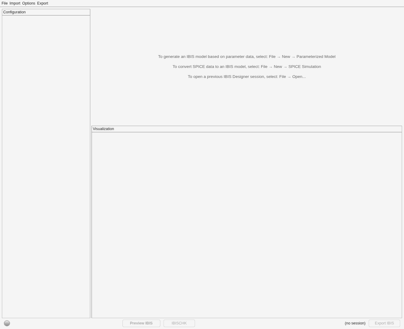
Select File > New > SPICE Simulation from the menu bar. The Load Simulation Files dialog is where you specify your input data. It opens automatically when creating a new session and can be reopened at any time via the Load Files button.
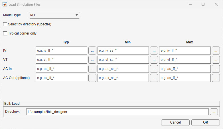
Load Simulation Files
The Load Simulation Files dialog has fields for the model type, dialog options, a simulation directory for bulk auto-fill, and individual file paths for each corner and file type.
Select the Model Type
Set the Model Type dropdown to I/O. This enables all file rows because an I/O buffer needs both driver data (IV, VT) and receiver data (AC for input capacitance). The model type determines which file rows are active:
Model Type | IV | VT | AC In | AC Out |
|---|---|---|---|---|
Input | disabled | disabled | required | disabled |
Output | required | required | required | optional |
I/O | required | required | required | optional |
Note: Additional model types are available from the Model Type dropdown to support many different applications.
Dialog Options
Below the Model Type dropdown, two check boxes control how files are selected:
Select by Directory: When checked, the individual browse buttons ("...") switch from file selection to directory selection. This is designed for Cadence Spectre users whose simulation output is organized as
.rawdirectories (one directory per simulation run) rather than individual files. When unchecked (the default), browse buttons open a file picker filtered by the appropriate extensions for that row (e.g.,.csvand.sw0for IV files).Typical corner only: When checked, the Min and Max columns are disabled and grayed out. The generated IBIS model will contain only typical-corner data (no min/max IV curves or VT waveforms). This is useful when you have simulation results at only one process corner and want to generate a preliminary model without waiting for full PVT characterization. The min/max corner temperature, voltage, and package RLC fields are also disabled.
For this example, leave both check boxes unchecked. We have full three-corner HSPICE data.
Use Auto-Fill to Load Files
Click the Browse button next to the Simulation directory field and navigate to the example directory containing the example simulation files. When you select the directory, IBIS Designer automatically scans for files matching the naming convention {file_type}_{corner}_{modelname}.{ext} and fills all file path fields.
The auto-fill recognizes these corner identifiers:
Typical:
tt,typ, ornomSlow (min):
ss,slow, orminFast (max):
ff,fast, ormax
After auto-fill completes, all 12 file fields are populated as shown in the screenshot below.
Browse for Individual Files
Alternatively, you can populate file paths one at a time using the "..." browse button next to each field. This is useful when your files do not follow the auto-fill naming convention, are spread across different directories, or when you need to override a single file that auto-fill assigned incorrectly. The file picker filters by extension based on the row type: IV rows show .csv and .sw0 files, VT rows show .csv and .tr0 files, and AC/AX rows show .csv and .ac0 files.
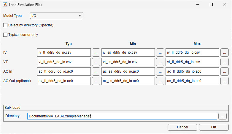
Click OK to accept the file assignments. The dialog closes and the main panel's corner table populates with the loaded file paths.
Configure Model Identity
Set the following fields in the IBIS Model section of the left panel:
Model Name:
ddr5_dq_io. This becomes the[Model]keyword in the IBIS file. Must be unique within the file. EDA tools reference this name when assigning models to pins.Component:
DDR5_PHY. This becomes the[Component]keyword, typically representing the chip or die that contains this buffer.Manufacturer:
Generic. Identifies the silicon vendor in the IBIS file header.Pin Number:
A1. The pin identifier that appears in the[Pin]table.Signal Name:
DQ0. The signal name associated with this pin.
These fields map directly to IBIS file keywords. When you later use this model in a signal integrity simulator, you reference it by the Model Name and associate it with physical pins via the Pin Number and Signal Name fields.
Differential Configuration
The Differential section provides an optional check box and fields for differential pin pairs. When the Differential check box is enabled, the generated IBIS file includes a two-pin [Pin] table and a [Diff Pin] section that pairs the non-inverting and inverting pins. The fields are:
Vdiff (V): The differential input voltage threshold written to the
[Diff Pin]table. Default is 0.1 V.Pin Numbers: Two fields specifying the pin identifiers for the positive and negative pins of the pair (e.g.,
A1andB1).Signal Names: Two fields specifying the signal names for each pin (e.g.,
DQ0_pandDQ0_n).
For this DDR5 single-ended DQ example, leave the Differential check box unchecked. Differential mode is used for signals like DQS (data strobe) or CK (clock) that are routed as complementary pairs.
Set Model Parameters
The Model Parameters section contains receiver thresholds and timing test load values that are written as subparameters of the [Model] keyword in the IBIS file. These parameters allow EDA tools to determine digital switching thresholds and to construct the correct test load for propagation delay measurements. Enter the following values:
Parameter | Value | Description |
|---|---|---|
Vinl (V) | 0.86 | Input logic low DC voltage; the voltage at or below which the receiver recognizes a logic 0 |
Vinh (V) | 1.06 | Input logic high DC voltage; the voltage at or above which the receiver recognizes a logic 1 |
Vmeas (V) | 0.96 | Timing measurement reference voltage; the threshold at which to measure propagation delay on the output waveform |
Vref (V) | 1.1 | Timing test load bias voltage; the DC voltage applied to the far end of Rref in the reference load circuit |
Rref (Ohm) | 50 | Timing test load resistance; the resistance used in the propagation delay measurement fixture |
Cref (F) | 10e-12 | Timing test load capacitance; the capacitance used in the propagation delay measurement fixture |
These values are specific to DDR5 DQ signaling. For other interface standards, consult the specification for the appropriate threshold and reference levels. If left blank (NaN), the corresponding subparameter is omitted from the IBIS file.
For advanced per-corner parameters (overshoot limits, hysteresis thresholds, edge-specific timing loads), use Options > IBIS Parameters from the menu bar. Those values are written to the [Model Spec] keyword, which can override the [Model]-level values on a per-corner basis. The defaults are sufficient for most applications.
Configure Corner Values
Set the operating conditions for each process corner in the Corner Values section. These values define the temperature and supply voltage that were used during input file generation and will appear in the generated IBIS file:
Corner | Temperature | Voltage | IBIS Meaning |
|---|---|---|---|
Typical | 25 degrees C | 1.1V | Nominal operating conditions |
Min (Slow) | 100 degrees C | 1.067V | Worst-case drive strength: high temperature, low voltage |
Max (Fast) | 0 degrees C | 1.166V | Maximum drive strength: low temperature, high voltage |
The IBIS "min" corner represents minimum drive strength (slowest buffer), not minimum voltage. This is why the slow corner has high temperature (increased carrier scattering reduces mobility) and low voltage (less overdrive).
Verify the Temperature values and update the Voltage values to match the table above.
Configure Package RLC
The Package RLC section specifies the parasitic resistance, inductance, and capacitance of the package interconnect between the die pad and the external pin. These values are written to the [Package] keyword in the IBIS file and allow the simulator to model package effects on signal integrity.
Each parameter has Typ, Min, and Max columns corresponding to the three process corners:
Parameter | Typ | Min | Max | Description |
|---|---|---|---|---|
R (Ohm) | 0.001e-3 | 0.001e-3 | 0.001e-3 | Series resistance of the package trace/bond wire |
L (H) | 1e-12 | 1e-12 | 1e-12 | Series inductance of the package trace/bond wire |
C (F) | 1e-15 | 1e-15 | 1e-15 | Shunt capacitance of the package pin pad to ground |
For this example, the Package RLC values are set to negligibly small defaults. In a production model, you would obtain these values from the package substrate design (e.g., from a 3D EM extraction tool) and they would vary across corners to reflect manufacturing tolerances. If Min and Max are left blank (NA), only the Typ column is written to the IBIS file.
Set Conversion Options (Optional)
IBIS Designer provides conversion options that control how raw simulation data is processed. For most use cases, the defaults produce correct results. Access these options via Options > Conversion Options from the menu bar.
The dialog is organized into two tabs: IV / VT (extraction parameters) and Edge Detection (transition identification algorithm).
Tab 1: IV / VT Options
The left panel contains IV extraction options:
Option | Default | Description |
|---|---|---|
Split IV Zero | Yes | Split the combined off-state clamp current into separate GND Clamp and Power Clamp tables at the zero-current crossing point. When "Yes" (default), the current below the zero-crossing is assigned to GND Clamp and the current above is assigned to Power Clamp. When "No", all clamp data goes into GND Clamp (with extended voltage range) and Power Clamp is written as a trivial zero table. |
Clamp IV | 1.0 A | Maximum allowable clamp current magnitude. Clamp IV data points exceeding this limit are clipped. Prevents unrealistic extrapolation in the IBIS file. |
IV Mono | Yes | Enforce monotonicity on Power Clamp IV curves (required by the IBIS specification). When "Yes", any non-monotonic data points are corrected by interpolation. |
Force IV 0 | No | When "Yes", collapses the zero-crossing range in the clamp IV curves to a single point. Improves model stability for simulators that are sensitive to near-zero current regions. |
The right panel contains VT / Ramp extraction options:
Option | Default | Description |
|---|---|---|
VT Time | (auto) | Override the automatically calculated maximum waveform time. Leave blank (NaN) to let IBIS Designer determine the endpoint from the simulation data settlement. Specify a value in seconds to manually truncate or extend the extracted waveform window. |
VT Start Time | 0 | Time offset (seconds) to skip at the beginning of the VT simulation. Useful for trimming initial transient settling artifacts before the stimulus edge arrives. |
VT Offset Typ/Min/Max | 0 / 0 / 0 | Per-corner time shift (seconds) applied to the extracted waveform start. Allows independent alignment of each corner's waveform if the stimulus timing differs between PVT simulations. |
VT Count | 4 | Number of VT waveforms to extract. "4" generates rising and falling waveforms into both GND-terminated and VDD-terminated fixtures. "2" generates rising and falling into GND fixture only. |
Ramp Offset | 0 | Time offset (seconds) for the dV/dt ramp calculation. Shifts the measurement window used to compute the 20%-to-80% rise/fall time. |
Tab 2: Edge Detection Options
These options control how IBIS Designer identifies rising and falling transitions in the VT simulation data. The Edge Mode dropdown selects the detection algorithm:
Standard (default): Automatically detects stimulus voltage levels, identifies edges using 20%/80% threshold crossings with hysteresis, and extracts the first rising and falling transitions. This mode works for clean simulation data, noisy or ringing waveforms, incomplete voltage swings, and multi-edge stimuli. All other options in this tab are grayed out because the defaults handle these cases.
Custom: Enables all options below for manual control. Use Custom mode when you need to extract a specific edge from a multi-pulse stimulus, override the automatically detected stimulus levels, adjust the detection thresholds, or add hold-time filtering for extremely noisy data.
When Edge Mode is set to Custom, the following options become available:
Option | Default | Description |
|---|---|---|
Rise Edge # | 1 | Which rising edge occurrence to extract (1 = first rising edge, 2 = second, etc.). Useful when the VT simulation contains multiple transitions and you need to select a specific one. |
Fall Edge # | (auto) | Which falling edge occurrence to extract. When blank, IBIS Designer automatically selects the first falling edge after the extracted rising edge. |
Thresh Low | 0.2 | Low threshold fraction (0 to 1) for edge detection. A transition is considered to have started when the signal crosses this fraction of the full voltage swing. |
Thresh High | 0.8 | High threshold fraction (0 to 1) for edge detection. A transition is considered complete when the signal crosses this fraction of the full voltage swing. |
Min Hold | 0 | Minimum hold time (seconds) that the signal must remain beyond a threshold before the crossing is accepted. Filters out brief glitches that might otherwise be detected as false edges. |
Stimulus Low | (auto) | Override the automatically detected low-state voltage of the stimulus signal. When blank, IBIS Designer infers this from the stimulus waveform data. |
Stimulus High | (auto) | Override the automatically detected high-state voltage of the stimulus signal. When blank, IBIS Designer infers this from the stimulus waveform data. |
For this example, leave Edge Mode set to Standard. The defaults are calibrated for standard DDR-style testbench configurations with a 50-ohm fixture, a single rising and falling edge per simulation, and 20%/80% threshold crossings for ramp calculation.
Preview IBIS
Click the Preview IBIS button in the action bar at the bottom of the window. The conversion pipeline performs these steps:
Validate inputs: Confirms all required files are present and parameters are consistent
Read simulation files: Parses CSV data (auto-detects format and column structure)
Extract IV curves: Separates the DC sweep data into Pulldown, Pullup, GND Clamp, and POWER Clamp curves using the Split_IV algorithm
Extract VT waveforms: Identifies rising and falling edges in the transient data, extracts the relevant time windows, and aligns them relative to the edge start
Extract C_comp: Computes die capacitance from the AC admittance:
Compute Ramp: Calculates dV/dt from the 20%-80% transition of the VT waveforms
Assemble model: Combines all extracted data into a complete IBIS model in memory
The status bar shows progress. When conversion finishes, the status lamp turns green and shows "Preview complete". The model is now in memory but has not been written to disk yet: 
Review Results
After preview, the Visualization panel at the bottom of the window populates with results. Use the tabs to inspect each aspect of the extracted model.
IV Curves
The IV Raw tab shows the IV curves extracted from each corner's DC sweep data. For an I/O buffer, six sub-tabs are available: Pulldown, Pullup, Pullup VR, Power Clamp, Power Clamp VR, and GND Clamp.
Pulldown: Current vs. pad voltage for the NMOS pull-down driver (ground-referenced). Shows the low-side drive strength extracted directly from the DC sweep.
Pullup: Current vs. pad voltage for the PMOS pull-up driver. The x-axis is converted from the Vcc-relative representation to absolute pad voltage (Vpad = Vcc - Vtable), making it easier to visualize where current flows relative to the supply rails.
Pullup VR: The same Pullup data plotted in its native voltage-relative form, exactly as it appears in the IBIS file. The x-axis is Vtable = Vcc - Vpad, so 0 V corresponds to the pad at Vcc. This is the format that IBIS simulators read directly.
Power Clamp: Current vs. pad voltage for the supply protection diode. Like the Pullup tab, the x-axis is converted from Vcc-relative to absolute pad voltage for intuitive visualization.
Power Clamp VR: The same Power Clamp data in its native voltage-relative form as stored in the IBIS file. The x-axis is Vtable = Vcc - Vpad.
GND Clamp: Current vs. pad voltage for the substrate protection diode, active when the pad voltage drops below ground. This curve is ground-referenced (x-axis is pad voltage directly), so no VR variant is needed.
Each curve shows typ (blue), min (green), and max (red) corners. The min corner shows reduced current at the same voltage (weaker drive due to higher resistance).
IV Combined
The IV Combined tab shows the total current that a signal integrity simulator would compute at the pad by summing the individual IV components. It has two sub-tabs:
Pulldown: Total output-low current: Pulldown IV + Power Clamp IV + GND Clamp IV, all interpolated to a common pad voltage grid from -Vcc to 2*Vcc.
Pullup: Total output-high current: Pullup IV + Power Clamp IV + GND Clamp IV, similarly interpolated to pad voltage.
These combined plots show what a receiver would see when the driver is in the low or high state. The clamp currents are negligible in the mid-range (between 0 and Vdd) but become significant near the rails, where the ESD clamp activates. Comparing the combined curves against the raw curves helps verify that the clamp and driver contributions interact correctly.
VT Waveforms
The VT Waveforms tab shows the transient voltage response extracted from the simulation. Four waveforms are generated (with VT_Count = 4), each shown in a sub-tab:
Rising (GND): Output transitions from low to high into a load terminated to ground.
Rising (Vdd): Output transitions from low to high into a load terminated to Vdd.
Falling (GND): Output transitions from high to low into a GND-terminated load.
Falling (Vdd): Output transitions from high to low into a VDD-terminated load.
Unlike the Parameterized Model workflow (which generates idealized RC transitions), these waveforms capture the actual nonlinear switching behavior of the transistor-level circuit, including any overshoot, undershoot, or non-monotonic settling.
IBIS Preview
The IBIS Preview tab shows the complete text of the generated IBIS file. Scroll through to verify the structure:
[IBIS Ver]header with version 6.1[Component]section with the configured component name, manufacturer, and pin table[Model]section with Model_type I/O, Vinh/Vinl, C_comp values, and all IV/VT data tablesRamp data (dV/dt for rising and falling edges, derived from the VT waveform 20%-80% transitions)
[End]keyword
Logs
The Logs tab records a timestamped run history showing validation status, extraction progress, and the results of ibischk validation (if enabled via Options > Always Run IBISCHK). When ibischk runs, the full output including any error or warning messages is appended here.
Validate with IBISCHK (Optional)
Before exporting, you can validate the generated model against the IBIS specification by clicking the IBISCHK button in the action bar. This step is optional and requires a Signal Integrity Toolbox license. If the toolbox is not installed, the button displays an alert indicating that ibischk is not available.
The ibischk validator is the industry-standard compliance checker maintained by the IBIS Open Forum. It parses the generated IBIS file and checks for:
Errors: Specification violations that would prevent a simulator from reading the file correctly (e.g., non-monotonic IV data, missing required keywords, out-of-range values). These must be fixed before distributing the model.
Warnings: Informational notes about unusual values or absent optional fields (e.g.,
[Model Spec]not present, package parasitics near zero). Warnings are typically acceptable and do not affect simulator interoperability.
Results appear in the Logs tab of the Visualization panel and in the status bar, which shows a summary such as "Done. ibischk: 0 errors, 2 warnings". If errors are found, the status lamp turns amber and shows "Done with issues."
You can also enable automatic validation after every preview by selecting Options > Always Run IBISCHK from the menu bar. When enabled, IBIS Designer runs ibischk each time you click Preview IBIS, so you get immediate feedback as you iterate on conversion options or corner parameters.
A valid model produced from clean simulation data should show zero errors. Warnings are common and usually informational (for example, noting that optional fields like [Model Spec] are not present).
Export the IBIS File
Click Export IBIS in the action bar to write the generated model to a .ibs file on disk. The file is saved to the Target directory specified in the Output section, using the filename from the IBIS Filename field in the IBIS Model section. If Target directory is blank, the current MATLAB working directory is used.
Save the Session
To preserve your work for later editing, save the session via File > Save (or File > Save As... to choose a new location). The session is stored as a .mat file (default name s2i_session.mat) that captures the complete app state:
All configuration panel settings (model identity, corner values, model parameters, package RLC)
Loaded file paths and simulation directory
Conversion options and results
Output directory and filename preferences
You can also use Export > Export to MATLAB to generate a standalone MATLAB script that recreates the current session programmatically. Unlike the session file (which stores internal app state), the exported script uses public API calls and is suitable for version control, automation, or batch processing.
Programmatic Equivalent
The entire workflow demonstrated above can be reproduced programmatically using the IBIS Designer public API. The following script converts the same DDR5 I/O dataset without opening the GUI:
dataDir = pwd;
Configure the Data Object
Create a data container and set the model identity, supply voltage, and corner-specific file paths:
d = ibisDesignerData;
d.ModelName = "ddr5_dq_io";
d.ModelType = "I/O";
d.ComponentName = "DDR5_PHY";
d.ManufacturerName = "Generic";
d.PinName = "A1";
d.SignalName = "DQ0";
d.Vdd = 1.1;
Assign Corner Data
Each corner needs a temperature, voltage, and file paths for IV, VT, and AC data:
d.CornerData(1).Corner = "typ";
d.CornerData(1).Temperature = 25;
d.CornerData(1).Voltage = 1.1;
d.CornerData(1).IVFile = fullfile(dataDir, "iv_tt_ddr5_dq_io.csv");
d.CornerData(1).VTFile = fullfile(dataDir, "vt_tt_ddr5_dq_io.csv");
d.CornerData(1).ACFile = fullfile(dataDir, "ac_tt_ddr5_dq_io.ac0");
d.CornerData(1).AXFile = fullfile(dataDir, "ax_tt_ddr5_dq_io.ac0");
d.CornerData(2).Corner = "min";
d.CornerData(2).Temperature = 100;
d.CornerData(2).Voltage = 1.067;
d.CornerData(2).IVFile = fullfile(dataDir, "iv_ss_ddr5_dq_io.csv");
d.CornerData(2).VTFile = fullfile(dataDir, "vt_ss_ddr5_dq_io.csv");
d.CornerData(2).ACFile = fullfile(dataDir, "ac_ss_ddr5_dq_io.ac0");
d.CornerData(2).AXFile = fullfile(dataDir, "ax_ss_ddr5_dq_io.ac0");
d.CornerData(3).Corner = "max";
d.CornerData(3).Temperature = 0;
d.CornerData(3).Voltage = 1.166;
d.CornerData(3).IVFile = fullfile(dataDir, "iv_ff_ddr5_dq_io.csv");
d.CornerData(3).VTFile = fullfile(dataDir, "vt_ff_ddr5_dq_io.csv");
d.CornerData(3).ACFile = fullfile(dataDir, "ac_ff_ddr5_dq_io.ac0");
d.CornerData(3).AXFile = fullfile(dataDir, "ax_ff_ddr5_dq_io.ac0");
Set Model Parameters
d.Vinl = 0.86;
d.Vinh = 1.06;
d.Vmeas = 0.96;
d.Vref = 1.1;
d.Rref = 50;
d.Cref = 10e-12;
Set Fixture and Package Parameters
d.RFixture = 50;
d.VFixtureGnd = 0;
d.PackageR = [0.001e-3, 0.001e-3, 0.001e-3];
d.PackageL = [1e-12, 1e-12, 1e-12];
d.PackageC = [1e-15, 1e-15, 1e-15];
Validate, Convert, and Write
The validate method checks that all required files exist and parameters are consistent. Then ibisProcessor runs the extraction pipeline and ibisWriter produces the output file:
d.validate();
converter = ibisProcessor(d);
ibisFile = ibisWriter(converter);
ibisFile.writeIBISFile("ddr5_dq_io.ibs");
Validate with IBISCHK
Run the ibischk compliance checker against the exported file (requires Signal Integrity Toolbox):
ibischk("ddr5_dq_io.ibs");The three-step pipeline (ibisDesignerData -> ibisProcessor -> ibisWriter) mirrors the GUI workflow exactly: configure, convert, export. The ibisProcessor call performs the same extraction as the Preview IBIS button, and ibisWriter formats and writes the same IBIS file content as Export IBIS.
Summary
This example demonstrated how to create an IBIS model from SPICE simulation data using the SPICE Simulation workflow in IBIS Designer. The key steps were:
Preparing simulation data in the required format (IV sweeps, VT transients, AC admittance for each process corner)
Using auto-fill to efficiently load all 12 files from a directory
Configuring corner parameters (temperature, voltage) to match simulation conditions
Running the conversion pipeline to extract IV curves, VT waveforms, C_comp, and Ramp
Reviewing the extracted results and exporting the validated IBIS file
Next steps:
For early-stage models when SPICE data is not yet available, see the Create IBIS Model from Electrical Specifications example.
To add multiple models to a single IBIS file (e.g., DQ, DQS, CA buffers for a complete DDR5 PHY), use the Append workflow: generate each model, then Import > Import IBIS File to merge them into one file.
Use Export Script in the GUI action bar to automatically generate a programmatic script from your current session configuration.
References
See Also
IBIS Designer | ibischk (Signal Integrity Toolbox)

