Histogram Equalization Using Video Frame Buffer
This example shows how to design a histogram equalization algorithm that uses HDMI input and output and external memory.
Video processing applications often store a full frame of video data to process the frame and modify the next frame. In such designs the video frames are stored in external memory and the FPGA design reads from memory and processes the video data in sections.
Supported hardware platforms (with FMC-HDMI-CAM mezzanine card)
Xilinx® Zynq® UltraScale+™ MPSoC ZCU106 Evaluation Kit
Xilinx Zynq UltraScale+ MPSoC ZCU102 Evaluation Kit
Xilinx Zynq ZC706 Evaluation Kit
Design Task and System Requirements
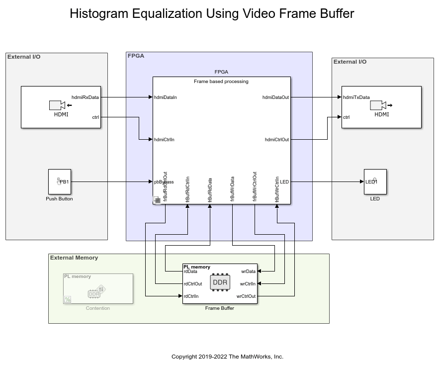
Consider an application involving continuous streaming of video data through the FPGA. In the top model soc_histogram_equalization_top, the FPGA subsystem calculates the histogram of the incoming video stream and writes the input video stream to external memory for storage. At the end of each frame, the design triggers a synchronization signal that starts read back of the stored frame from external memory. The design performs equalization by applying the accumulated histogram vector to the video stream as it is read back from external memory. The AXI4 Video Frame Buffer block models the external memory frame buffer.
The HDMI Input block reads a video file and provides video data and control signals to downstream FPGA processing blocks. Video data is in YCbCr 4:2:2 format, and the control signals are in the pixel control bus format. The HDMI Output block reads video data and control signals, in the same format as output by the HDMI Input block, and provides a visual output using the Video Display block.
The Push Button block enables bypassing of the histogram equalization algorithm, by routing the unprocessed output from the external memory frame buffer to the output.

Consider these requirements when designing an application that interfaces with external memory:
Throughput: What is the rate that you need to transfer data to/from memory to satisfy the requirements of your algorithm? Specifically for vision applications, what is the frame-size and frame-rate that you must be able to maintain?
Latency: What is the maximum amount of time that your algorithm can tolerate between requesting and receiving data? For vision applications, do you need a continuous stream of data, without gaps? Are you able to buffer samples internal to your algorithm in order to prevent data loss when access to the memory is blocked?
This histogram equalization example meets the following requirements:
Throughput must be sufficient to maintain a 1920x1080p video stream at 60 frames-per-second.
Latency must be sufficiently low so as not to drop frames.
To meet the video throughput requirement, the frame buffer throughput must satisfy this equation.

Because the video format is YCbCr 4:2:2, it uses 2 bytes-per-pixel (BPP) and results in a throughput requirement of

The algorithm must both write and read each frame to/from the external memory, so the throughput requirement must be doubled, for a total throughput requirement of

Design Using SoC Blockset
In general, your algorithm will be a part of a larger SoC application. In such applications, it is likely that there will be other algorithms also requiring access to external memory. In this scenario, you must consider the impact of other algorithm's memory accesses on the performance and requirements of your algorithm. Assuming that your algorithm shares the memory channel with other components, you should consider the following:
What is the total available memory bandwidth in the SoC system?
How will your algorithm adapt to shared memory bandwidth?
Can your algorithm tolerate an increased read/write latency?
By appropriate modeling of additional memory consumers in the overall application, you can systematically design your algorithm to meet your requirements in situations where access to the memory is not exclusive to your algorithm.
To avoid modeling of all memory readers and writers in the overall system, you can use Memory Traffic Generator blocks to consume read/write bandwidth in your system by creating access requests. In this way, you can simulate additional memory accesses within your system without explicit modeling.
Modeling Additional Memory Consumers
Simulate the system without additional memory consumers and view the memory performance plot on the Performance App:
On the Simulink Toolstrip, on the System on Chip tab, click Performance Report.
In the Report Browser pane, navigate to
Memory Utilization/PL Memory Controller.In the Controls pane, set Select plot type to
Bandwidth, and select both masters to plot.Click Create Plot.

The memory masters are configured as follows:
Master 1: Frame Buffer write
Master 2: Frame Buffer read
Master 3: Contention - commented out
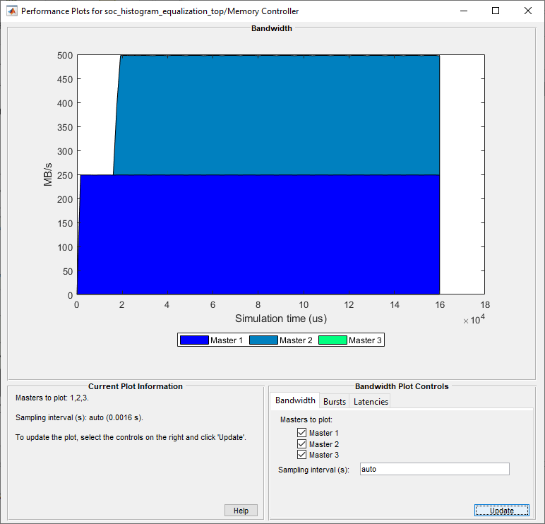
Note that both active masters are consuming 248.8 MB/s of memory bandwidth.
More Memory Consumers: Consider that your algorithm is part of a larger system, and a secondary algorithm is being developed by a colleague or third-party. In this scenario, the secondary algorithm will be developed separately for the interest of time and division of work. Rather than combine the two algorithms into a single simulation, you can model the memory access of the secondary algorithm using a Memory Traffic Generator, and simulate the impact, if any, that it will have on your algorithm.
For example, assume that you are provided with the following memory requirements for the secondary algorithm:
Throughput: 1150 MB/s
Given that the primary algorithm consumes ~500 MB/s of the memory bandwidth, and the total available memory bandwidth is 1600 MB/s, we know that the total bandwidth requirement for our system exceeds the total available bandwidth by ~50 MB/s.
To enable the modeling of the secondary algorithm memory access, uncomment the Contention Memory Traffic Generator block. The block mask settings are shown below.

Simulating the system with the secondary algorithm's memory accesses, results in the following Memory Bandwidth Usage plot.

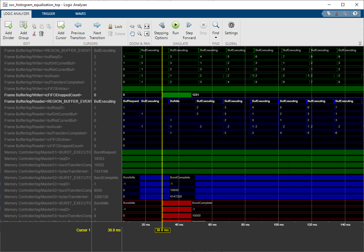
As you can see, at around 0.03s - when the secondary algorithm begins memory access requests, the other masters do not achieve their required throughput. The logic analyzer waveform shows this effect as dropped buffers for the Frame Buffer write master and the idle state for the Frame Buffer read master.

Implement and Run on Hardware
Following products are required for this section:
HDL Coder™
SoC Blockset™ Support Package for AMD® FPGA and SoC Devices. For more information about the support package, see SoC Blockset Supported Hardware
To implement the model on a supported SoC board use the SoC Builder tool. Open the mask of FPGA subsystem and set Model variant to Pixel based processing.
Comment out the Contention block.
To open SoC Builder, in the Simulink® toolstrip, on the System on Chip tab, click Configure, Build, & Deploy.
On the Setup screen, select Build model. Click Next.
On the Select Build Action screen, select Build, load, and run. Click Next.
On the Select Project Folder screen, specify the project folder. Click Next.
On the Review Memory Map screen, view the memory map by clicking View/Edit. Click Next.
On the Validate Model screen, check the compatibility of the model for implementation by clicking Validate. Click Next.
On the Build Model screen, begin building the model by clicking Build. An external shell opens when FPGA synthesis begins. Click Next.
On the Load Bitstream screen, click Next.
The FPGA synthesis can take more than 30 minutes to complete. To save time, you may want to use the provided pre-generated bitstream by following these steps:
Close the external shell to terminate synthesis.
Copy pre-generated bitstream to your project folder by running this command.
copyfile(fullfile(matlabshared.supportpkg.getSupportPackageRoot,'toolbox','soc',...
         'supportpackages','xilinxsoc','xilinxsocexamples','bitstreams',...
         'soc_histogram_equalization_top-zc706.bit'), './soc_prj');
Load pre-generated bitstream and run the model on the SoC board by clicking Load and Run.
Now the model is running on hardware. To get the memory bandwidth usage in hardware, execute the following axi-manager test bench for soc_histogram_equalization_top_aximanager.
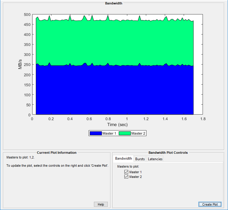
Once the execution ends, a plot window opens. Click Create plot and select both masters in the Bandwidth tab. Click Update.
The following figure shows the Memory Bandwidth usage when the application is deployed on hardware.

See Also
AXI4 Video Frame Buffer | Memory Traffic Generator | HDMI Tx | HDMI Rx