Vertical Video Flipping Using External Memory
This example shows how to design an application to flip an incoming video stream vertically.
You will use external memory to store a video frame to accomplish this task. You can use this technique for designing and implementing other vision applications requiring access to the external memory.
Supported hardware platform
Xilinx® Zynq® ZC706 evaluation kit + FMC-HDMI-CAM mezzanine card
Introduction
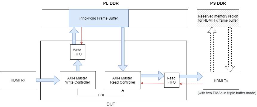
To flip the incoming video stream from HDMI source (RX), the FPGA logic writes the video frames a line at a time to the external memory. Later, the FPGA logic reads the stored image back, a line at a time in the reverse order, thus flipping the image vertically. The read video frame is then sent to the HDMI Out (TX). Video frames are stored in a ping-pong buffer in the PL-DDR, which enables independent memory write and read operations. A separate, PS-DDR is used for storing video frames during transfer of data to the HDMI Out. The diagram below highlights the overall data flow.
Modeling
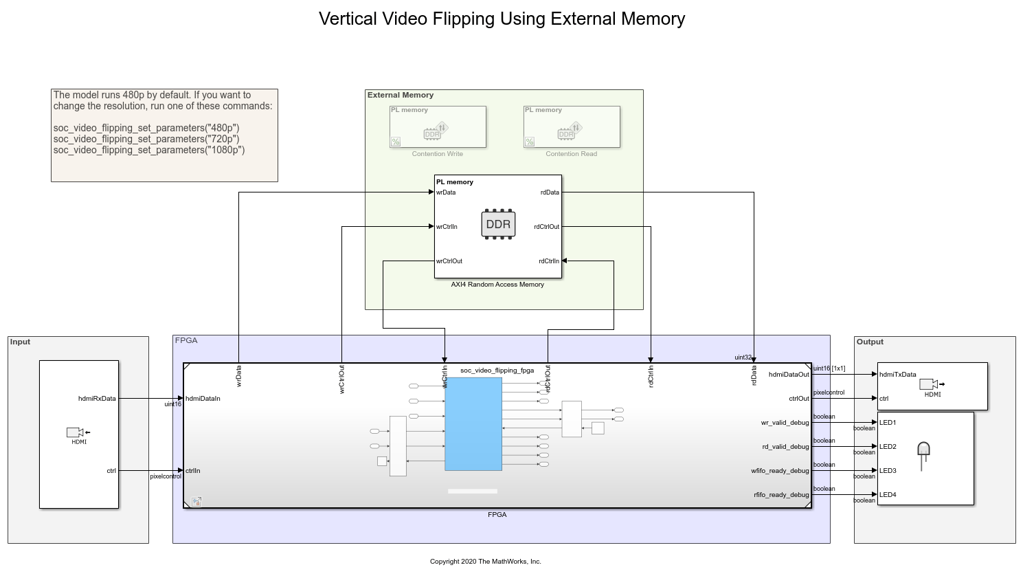
In the top model, soc_video_flipping_top.slx the FPGA logic is connected with the external memory and the HDMI In/Out blocks.
The soc_video_flipping_fpga.slx model includes the FPGA logic. It is linked as a referenced model from the top model. This image shows the contents of the VideoFlipping subsystem inside the soc_video_flipping_fpga model.
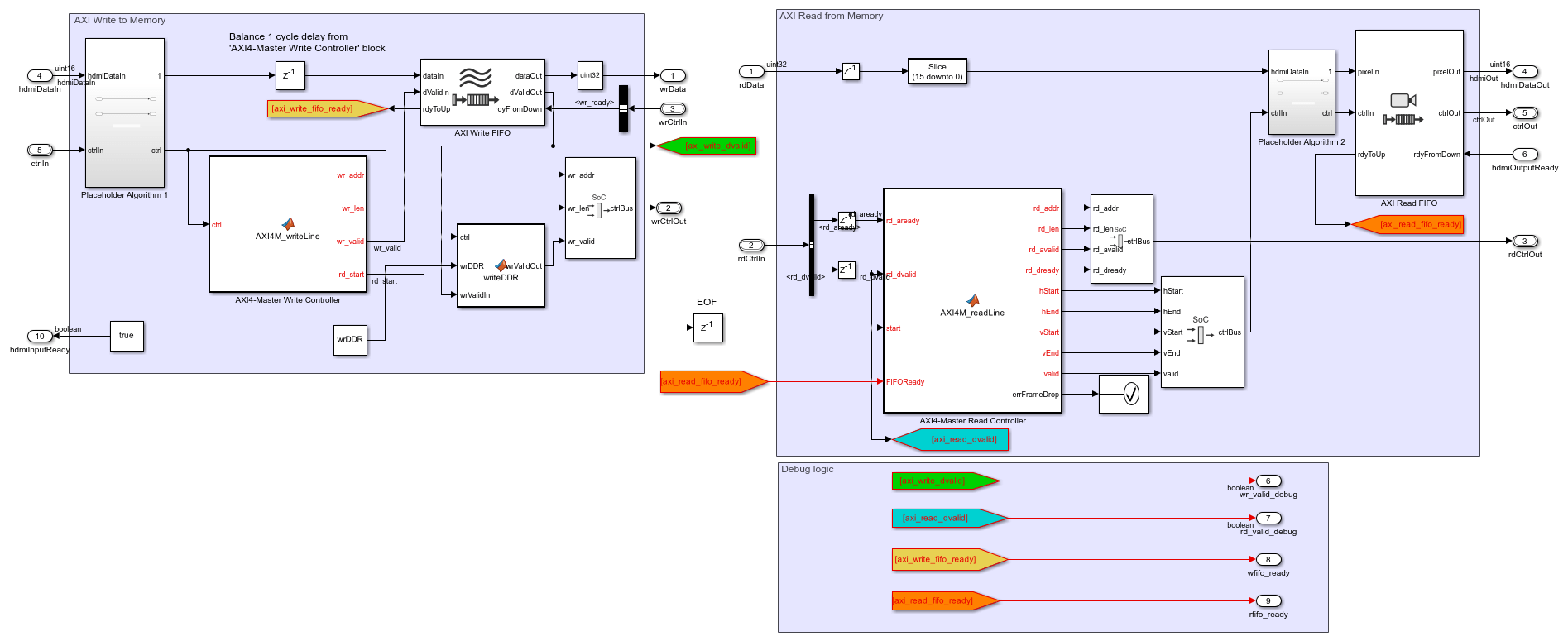
The FPGA logic consists of four key components:
AXI4 Master Write Controller receives video from HDMI Rx and writes the data into DDR. One line of data is written per burst. When one frame finishes, it sends the end of frame (EOF) signal to trigger AXI4 Master Read Controller.
AXI4 Master Read Controller reads the lines of the video frame from the external memory ping-pong buffer in reverse order. One line of data is read per burst. New read requests are paused if the downstream Read FIFO block is not ready to process data. When a frame is fully read from memory, the Read Controller waits for the next EOF signal from the Write Controller to start reading in a new frame. If the memory controller doesn't have enough bandwidth, the read controller may be still processing the earlier frame when the write controller finishes writing in the next frame. In this case, the Read Controller will throw an error using errFrameDrop signal.
Write FIFO buffers the data written to the ping-pong buffer when the DDR memory controller asserts the backpressure signal (highlighted red arrow), to allow video data from HDMI source to be processed. The Write FIFO should be large enough to prevent overflow and accommodate any delay in writing to the external memory. In this example the depth of the Write FIFO is set to 2048 to accommodate 1 HD line of backpressure.
Read FIFO buffers the data from the Read Controller when the DMA in the HDMI Tx asserts the backpressure signal (highlighted red arrow). The backpressure is propagated to the upstream AXI4 Master Read Controller to stop requesting data from DDR. Notice that since the AXI4 Master Read Controller will not pause during the read burst, it is important to make sure that the Read FIFO has enough room to store data even after its ready signal de-asserts. In this example, the depth of the Read FIFO is set to 2048 and the almost full threshold is set to 128. When the FIFO has 128 samples, the Read FIFO sends 'Full' signal to upstream block to stop any new read requests. In the meanwhile, it can buffer 2048-128 = 1920 samples without an overflow. The setting is sufficient even for a 1080p frame.
In the hardware implementation, the HDMI Tx includes two DMA frame buffers and one video timing controller (VTC), for robust and tear free video output. The DMAs may send backpressure to DUT when the memory controller is busy with other read or write transactions. In the FPGA model, the backpressure signal hdmiOutputReady is set to always true for simulation only (which indicates that the memory controller is always available). In practice, this signal often toggles between high and low. The Read FIFO block in the DUT is used to handle this backpressure.
Simulation
The memory bandwidth requirement must be considered when designing an application that interfaces with external memory. What is the rate that you need to transfer data to/from memory to satisfy the requirements of your algorithm? Specifically, for vision applications, what is the frame-size and frame-rate that you must be able to maintain?
For the selected ZC706 board, PL DDR controller is configured with 64-bit AXI4-Slave interface running at 200 MHz. The resulting bandwidth is 1600 MB/s. Let's first evaluate if the memory bandwidth is sufficient to maintain a 1920x1080p video stream at 60 frames-per-second. As the video format is YCbCr 4:2:2, we require 2 bytes-per-pixel. However, for the DUT AXI4 read and write, each pixel is zero-padded to 4 bytes, this equates to a throughput requirement of

The calculated throughput satisfies the bandwidth requirement.
To simulate 1080p 60fps case, run the following command and then simulate the model
soc_video_flipping_set_parameters("1080p")
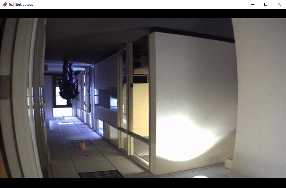
The output is shown as below.
If you want to model another DUT accessing the same external memory, you can use memory traffic generator block to simulate the contention before the implementation, so you can save effort on hardware debugging. In this model, two memory traffic generator blocks, Contention Write and Contention Read block, are modeled to mimic the AXI transactions of another frame buffer. The throughput of two memory traffic generators is calculated as

The total required bandwidth of memory controller is  Which is less than its maximum bandwidth 1600 MB/s. Uncomment Contention Write and Contention Read block, simulate the model for 1080P again, the output is torn at the bottom. You will also get assertion by 'soc_video_flipping_fpga/VideoFlipping/Assertion' block that frame get dropped.
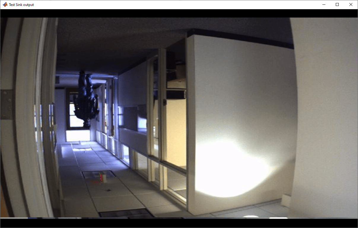
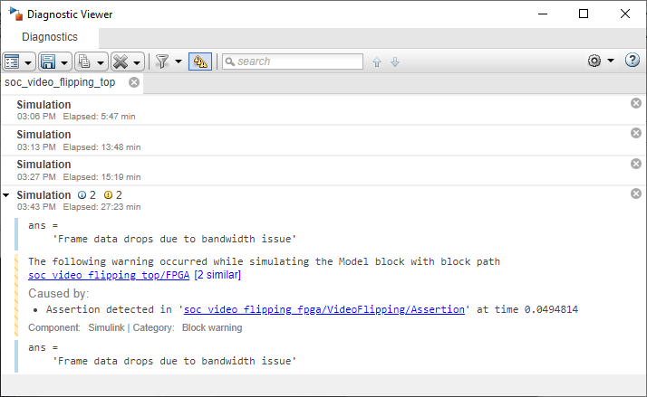
Simulation shows that memory controller can not meet the bandwidth requirement for the DUT and memory traffic generators. You may need to consider reducing the frame resolution, or making DUT algorithm more efficient, for example implementing pack/unpack 16bit YCbCr pixel to 32bit, other than zero padding.
The top model runs in Accelerator mode by default. If you want to inspect the logged data in Logic Analyzer, change the top model to Normal mode. It is best to simulate with 480p or smaller frame size for faster results.

Implementation
Following products are required for this section:
HDL Coder™
Before implementation,
Set the simulation mode to 'Normal' on the top model.
Comment out
Contention WriteandContention Readblocks.Run this command if the model has been changed for the frame size other than 1080p.
soc_video_flipping_set_parameters("1080p")
To implement the model on a supported SoC board use the SoC Builder tool. Make sure you have installed required products and FPGA vendor software before implementation. To open SoC Builder click, Configure, Build, & Deploy button in the toolstrip and follow these steps:
On the Setup screen, select Build model. Click Next.
On the Select Build Action screen, select Build, load and run. Click Next.
On the Select Project Folder screen, specify the project folder. Click Next.
On the Review Memory Map screen, to view the memory map, click View/Edit. Click Next.
On the Validate Model screen, to check the compatibility of the model for implementation, click Validate. Click Next.
On the Build Model screen, to build the model, click Build. An external shell opens when FPGA synthesis begins. Click Next.
On the Connect Hardware screen, to test the connectivity of the host computer with the SoC board, click Test Connection. To go to the Run Application screen, click Next.
The FPGA synthesis often takes more than 30 minutes to complete. To save time, you can use the provided pregenerated bitstream by following these steps.
Close the external shell to terminate synthesis.
Copy pregenerated bitstream to your project folder by running this
copyfilecommand below.Load the pregenerated bitstream and run the model on the SoC board by clicking Load and Run.
copyfile(fullfile(matlabshared.supportpkg.getSupportPackageRoot, ...
 'toolbox','soc','supportpackages','xilinxsoc','xilinxsocexamples', ...
 'bitstreams','soc_video_flipping_top-zc706.bit'),'./soc_prj');
The host computer can set parameters by writing to AXI4-Lite registers within the algorithm IP core by using the generated interface script named gs_soc_video_flipping_top_interface. The script includes this code that sets the wrDDR to true.
writePort(hFPGA, "wrDDR", 1);
Four LEDs on the ZC706 are driven by signals and can be used for debugging the design:
GPIO_LED_LEFT is driven by AXI4 Master write data valid. It should be on or blinking when the application is running.
GPIO_LED_CENTER is driven by AXI4 Master read data valid. It should be on or blinking when the application is running.
GPIO_LED_RIGHT is driven by Write FIFO ready. It should be always on, otherwise AXI4 Write data get dropped.
GPIO_LED_0 is driven by Read FIFO ready. It could be on or off. The data won't get dropped in this FIFO because the upstream controller will handle this backpressure properly.
Conclusion
This example shows modeling of AXI4 Master interfaces for accessing external memory in random fashion using SoC Blockset. You can use this technique to model vision applications involving external memory. One such example is Contrast Limited Adaptive Histogram Equalization with External Memory which builds further on this example.
See Also
HDMI Rx | HDMI Tx | AXI4 Random Access Memory