Import Custom HDL IP into SoC Blockset Design
This example shows how to import an HDL IP and integrate it into an SoC Blockset™ design. In this example, you import the Xilinx® Aurora IP as a Simulink® block and integrate it into a design. You simulate, build and deploy a system that generates and transmits a sinusoidal tone serially using Aurora hardware that first receives the signal from an RF channel. You then loop back the data and visualize the received tone by using an embedded processor.
Design Task
In this example, you import and integrate a Xilinx Aurora IP into a wireless system and implement the system on a Xilinx RFSoC device.
To add Xilinx Aurora IP to the generated Vivado® design, create a block that is compatible with an SoC Blockset design.
Import HDL IP Using HDL IP Importer
Import a Xilinx Aurora IP as a Simulink block and integrate it into an SoC Blockset design. Connect a FIFO at both the ends of the Aurora IP. The IP requires the input and output streaming data to run at a clock rate provided by the IP, which is different from the DUT clock. Package all the IPs as the single IP using the Xilinx Vivado IP Packager.
1. To open the HDL IP Importer tool, select HDL IP Importer on the System on Chip tab. Alternatively, enter hdlIPImporter at the MATLAB® command prompt.
2. On the Enter Block Details screen, specify the block name, library name, and library location. Click Next. For this example, specify Block name as Aurora 64B66B and Library name as socauroralib.
3. On the Select HDL IP Source Location screen, select Specify HDL IP source location and specify IP location as the output of this command. Click Next.
fullfile(matlabshared.supportpkg.getSupportPackageRoot,'toolbox','soc','supportpackages','xilinxsoc','blocks','auroraipsrc')
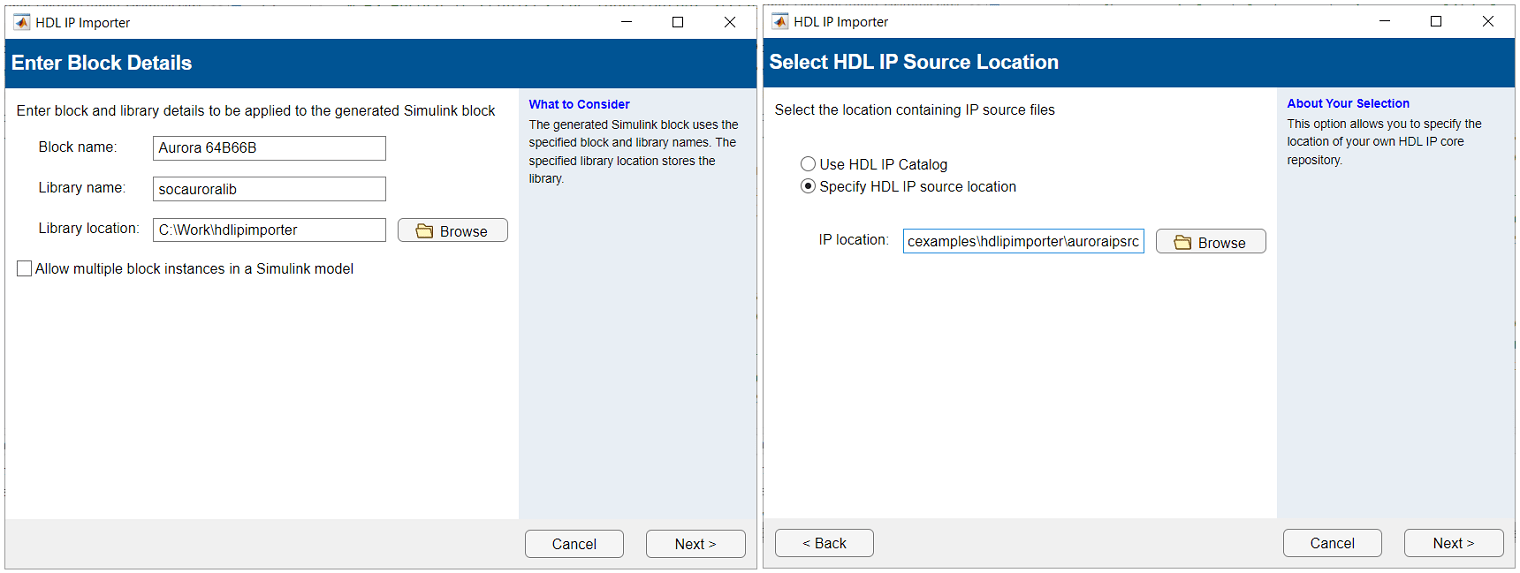
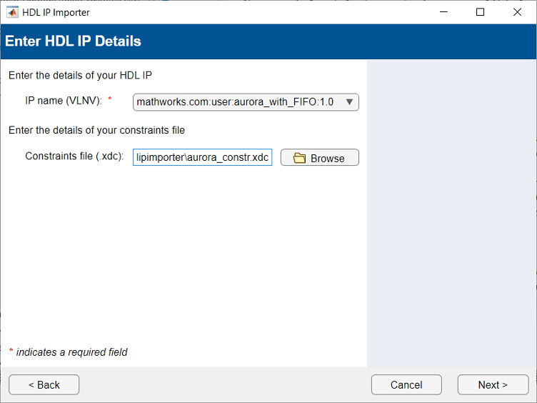
4. On the Enter HDL IP Details screen, specify Constraints file (.xdc) as the output of this command. This file defines the pins for the input reference clock. Click Next.
fullfile(matlabshared.supportpkg.getSupportPackageRoot,'toolbox','soc','supportpackages','xilinxsoc','blocks','aurora_constr.xdc')
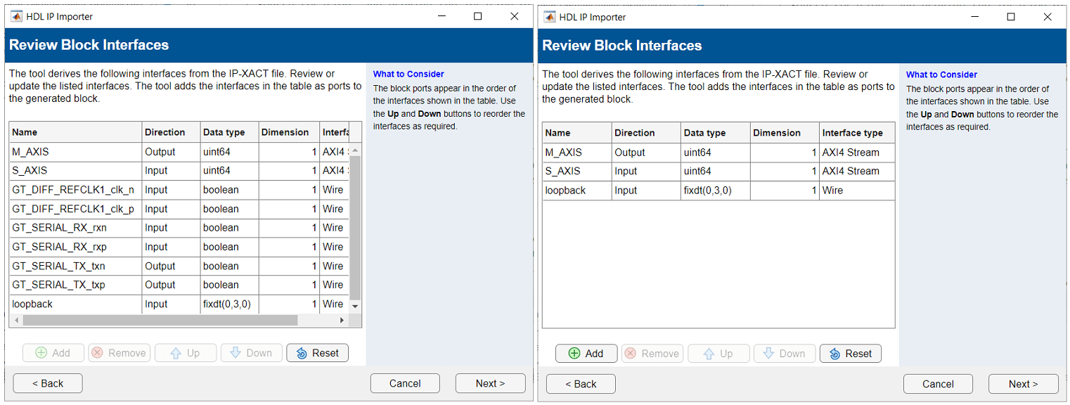
5. On the Review Block Interfaces screen, select the block interface rows in the table with the names GT_DIFF_REFCLK1_clk_n, GT_DIFF_REFCLK1_clk_p, GT_SERIAL_RX_rxn, GT_SERIAL_RX_rxp, GT_SERIAL_RX_txn, and GT_SERIAL_RX_txp, then click Remove. You must delete these interfaces because they are connected to external pins in the generated design. Click Next.
6. On the Review Clock and Reset Interfaces screen, for the init_clk interface, set Source to Register configuration. Click Next.
7. On the Enter Linux Device Details screen, click Next.
8. On the Summary screen, review the details in the table and click Generate.
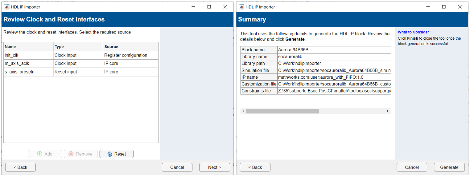
These steps create the Aurora 64B66B library block in the socauroralib library. The block has one input stream interface (S_AXIS) and one output stream interface (M_AXIS). The block also has a loopback input port, which you can use to loop back the data.
During block creation, the HDL IP Importer tool generates the socauroralib_Aurora64B66B_sim function. You can use this function to add behavioral simulation to the created block. In this example, you modify the function to include the pass-through logic.
function [M_AXIS_wrData,M_AXIS_wrValid,M_AXIS_wrLast,S_AXIS_rdReady] = socauroralib_Aurora64B66B_sim(M_AXIS_wrReady,S_AXIS_rdData,S_AXIS_rdValid,S_AXIS_rdLast,loopback,varargin) %#ok<INUSD>
%#codegen
%#ok<*EMCA>
M_AXIS_wrData = S_AXIS_rdData;
M_AXIS_wrValid = S_AXIS_rdValid;
M_AXIS_wrLast = S_AXIS_rdLast;
S_AXIS_rdReady = M_AXIS_wrReady;
end
The HDL IP Importer tool also generates the socauroralib_Aurora64B66B_customize TCL template. You can use this template to customize the HDL IP by configuring the HDL parameters and to make connections to the external I/O. In this example, you modify the TCL script to include the HDL IP connections to the external I/O.
proc socauroralib_Aurora64B66B_customize {ip_instance_name} {# Create interface ports
set GT_DIFF_REFCLK1 [ create_bd_intf_port -mode Slave -vlnv xilinx.com:interface:diff_clock_rtl:1.0 GT_DIFF_REFCLK1 ]
set_property -dict [ list \
CONFIG.FREQ_HZ {156250000} \
] $GT_DIFF_REFCLK1set GT_SERIAL_RX [ create_bd_intf_port -mode Slave -vlnv xilinx.com:display_aurora:GT_Serial_Transceiver_Pins_RX_rtl:1.0 GT_SERIAL_RX ]
set GT_SERIAL_TX [ create_bd_intf_port -mode Master -vlnv xilinx.com:display_aurora:GT_Serial_Transceiver_Pins_TX_rtl:1.0 GT_SERIAL_TX ]
# Create interface connections
connect_bd_intf_net [get_bd_intf_ports GT_DIFF_REFCLK1] [get_bd_intf_pins $ip_instance_name/GT_DIFF_REFCLK1]
connect_bd_intf_net [get_bd_intf_ports GT_SERIAL_RX] [get_bd_intf_pins $ip_instance_name/GT_SERIAL_RX]
connect_bd_intf_net [get_bd_intf_ports GT_SERIAL_TX] [get_bd_intf_pins $ip_instance_name/GT_SERIAL_TX]
}
This figure shows the block.

Design Model
This example follows the same design specifications as the Transmit and Receive Tone Using AMD RFSoC Device - Part 1 System Design example. Simulate the design before implementation by modeling the system using the RF Data Converter block, imported HDL IP block, and external memory blocks. Simulating the design enables you to identify and fix any issues in the Simulink model before implementation on the hardware.
Create an SoC model named soc_aurora_top as the top model and set the Hardware Board parameter to Xilinx Zynq UltraScale+ RFSoC ZCU111 Evaluation Kit. This model includes the soc_aurora_fpga FPGA model and the soc_aurora_proc processor model instantiated as model references. The top model also includes AXI4-Stream to Software block that shares the external memory between the FPGA and the processor. The FPGA model contains the imported HDL IP block.
open_system('soc_aurora_top')

close_system('soc_aurora_top')
Hardware Logic Design
To integrate the Xilinx Aurora IP into the SoC design, add the Aurora 64B66B block to the FPGA model. Use this block to transmit and receive the data serially on the hardware. For simulation, the block acts as a pass-through using a stream interface.
Use the loopback port to loop back the data on the hardware. The model controls the port from the processor through the ADC Capture subsystem by using an IP Core Register Read block.
The soc_aurora_fpga FPGA model contains three subsystems and one imported HDL IP block. The DAC Tone Generation subsystem connects to the DAC portion of the RFDC block and the ADC Capture subsystem connects to the ADC portion. The model generates four consecutive samples of the sinusoidal waveform in parallel by using an HDL-optimized NCO block. The output of the ADC Capture subsystem connects to the Aurora 64B66B (imported HDL IP) block, and its output connects to the Write To Processor subsystem.
The Write To Processor subsystem downsamples the data by a factor of 128 before sending it to the processor.
open_system('soc_aurora_fpga')

close_system('soc_aurora_fpga')
Processor Logic Design
The processor logic contains an event-based task driven by the arrival of data from the FPGA through DDR memory. The event-driven processor algorithm task corresponds to the dataTask port in the Task Manager block. The Task Manager block schedules data asynchronously by using a buffer ready event rdEvent in the memory. The event corresponds to the arrival of a data frame from the FPGA. The Processor Algorithm Wrapper subsystem in the soc_rfsoc_datacapture_proc processor model implements the algorithm and connects it to the Task Manager block at the top level. Because the model receives the data as a frame of four samples with the uint64 data type, you must first unpack and restore the sign of the data. The Processor subsystem then connects the output to Spectrum Analyzer and Scope blocks for visualization. The Initialize Function subsystem initializes several registers on the FPGA subsystems with their default values. Use the LoopbackVal variable in the MATLAB workspace to enable or disable the internal loop back. To disable the internal loop back, set this variable to 0. To enable the internal loop back, set this variable to 2.
open_system('soc_aurora_proc')

close_system('soc_aurora_proc')
Send and Receive Sinusoidal Tone
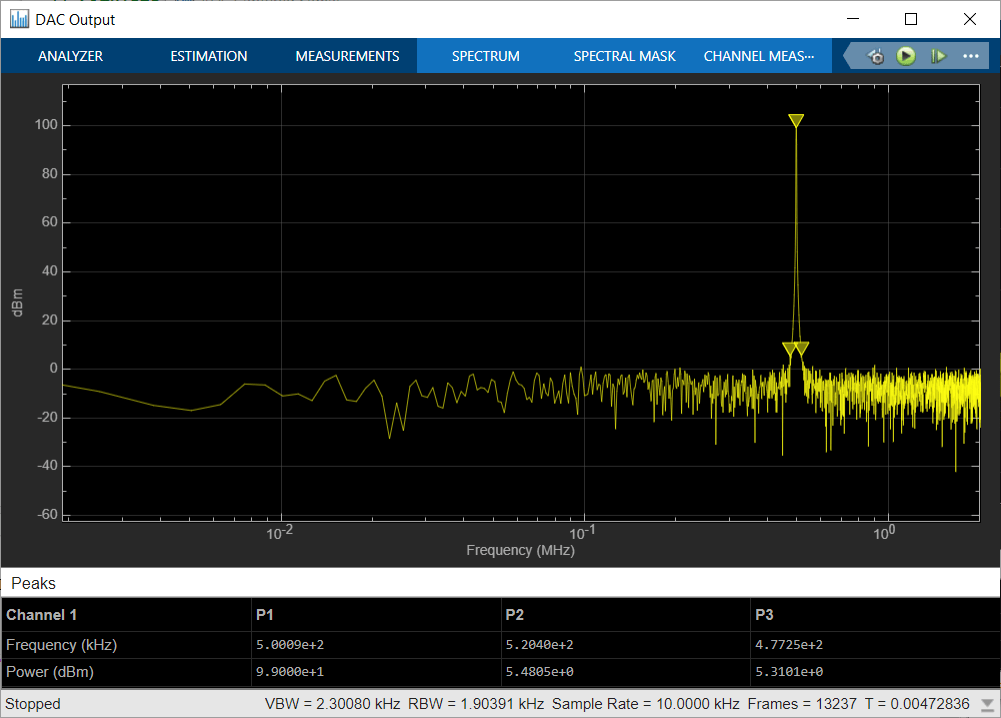
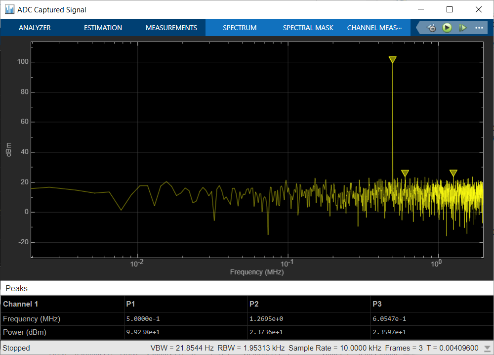
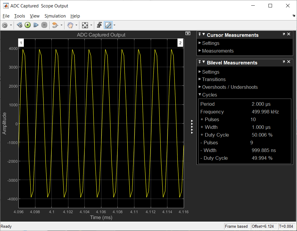
Run the model and visualize the sinusoidal tone generated from the FPGA. The system loops the waveform back from the FPGA to the processor through the RFDC block, the ADC Capture subsystem, the Aurora 64B66B block, and the Write To Processor subsystem in the FPGA and memory blocks. Use the processor system to visualize the waveform in the frequency domain using a Spectrum Analyzer block titled ADC Captured Signal. You can also visualize the signal in the time domain using a Scope block titled ADC Captured Scope Output. Because the path over which the data loops back is very long, the plots display the signals with a substantial delay. The transmitted and received signals show a tone of 0.5 MHz.
Implement and Run on Hardware
You can deploy this model to the Xilinx Zynq® UltraScale®+ ZCU111 evaluation kit with a XM500 Balun card.
Hardware Setup for ZCU111 Kit
Connect the SMA connectors on the XM500 Balun card to complete the loop back between the DACs and ADCs according to the connections in this table. Use DC blocks to loop back over differential channels.

To implement the soc_aurora_top model on the supported SoC board, use the SoC Builder tool. Set the Hardware Board option to Xilinx Zynq UltraScale+ RFSoC ZCU111 Evaluation Kit on the System on Chip tab of the Simulink toolstrip.
To open SoC Builder, click Configure, Build, & Deploy, and then follow these steps:
On the Setup screen, select Build model. Click Next.
On the Select Build Action screen, select Build and load for external mode. Click Next.
On the Select Project Folder screen, specify the project folder. Click Next.
On the Configure FPGA Parameters screen, review the FPGA parameter settings, and edit them if you need to. Click Next.
On the Review Hardware Mapping screen, to view the memory map, click View/Edit. Click Next.
On the Validate Model screen, to check the compatibility of the model for implementation, click Validate. Click Next.
On the Build Model screen, to build the model, click Build. An external shell opens when FPGA synthesis begins. Click Next.
On the Connect Hardware screen, to test the connectivity of the host computer with the SoC board, click Test Connection. To go to the Run Application screen, click Next.
The FPGA synthesis often takes more than 30 minutes to complete. To save time, you can use a pregenerated bitstream by following these steps.
Close the external shell to terminate synthesis.
Copy the pregenerated bitstream to your project folder by entering this command at the MATLAB command prompt.
copyfile(fullfile(matlabshared.supportpkg.getSupportPackageRoot, ...
 'toolbox','soc','supportpackages','xilinxsoc','xilinxsocexamples', ...
 'bitstreams','soc_aurora_top-XilinxZynqUltraScale_RFSoCZCU111EvaluationKit.bit'),'./soc_prj');
Load the pregenerated bitstream and run the model on the SoC board by clicking Load and Run.
After you load the bit file, open the generated software model, copy the Spectrum Analyzer and Scope blocks from the top model, and connect them to the Rate Transition block, as this figure shows. When you run the model, the Spectrum Analyzer shows the tone frequency of the received signal.

Run the model in external mode and verify that the frequency of the received tone is 0.5 MHz on the Spectrum Analyzer block.
Summary
In this example, you import an existing HDL IP as a Simulink block and integrate it into an SoC Blockset design. You integrate an HDL IP into a wireless system and simulate the system. Using SoC Builder, you implement the system and perform the loop back through Aurora hardware. Finally, you verify that the system behaves according to your needs.