Dual Rate Dual Port RAM
Dual Port RAM that supports two rates
Libraries:
HDL Coder /
HDL RAMs
Description
The Dual Rate Dual Port RAM block models a RAM that supports simultaneous read and write operations to different addresses at two clock rates. Port A of the RAM can run at one rate, and port B can run at a different rate.
In high-performance hardware applications, you can use this block to access the RAM twice per clock cycle. If you generate HDL code, this block maps to a dual-clock dual-port RAM in most FPGAs.
Simultaneous Access
You can access different addresses from ports A and B simultaneously. You can also read the same address from ports A and B simultaneously.
However, do not access an address from one RAM port while it is being written from the other RAM port. During simulation, if you access an address from one RAM port at the same time as you write that address from the other RAM port, the software reports an error.
Read-During-Write Behavior
The RAM has write-first behavior. When you write to the RAM, the new write data is immediately available at the output port.
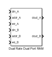
Ports
Input
din_A — Port A write data input
Scalar
(default)
Data that you write into the RAM memory location when we_A
is
true. The data inherits the width and data type from the input signal.
din_A
can be a double
,
single
, integer
, or a fixed-point
(fi)
object, and can be real or complex.
Data type: scalar fixed point, integer, or complex
Data Types: int8
| int16
| int32
| int64
| uint8
| uint16
| uint32
| uint64
| fixed point
addr_A — Port A write address
Scalar
(default)
Address that you write the data into when we_A
is true. This
value can be either fixed-point(fi)
or integer
,
must be unsigned, and have a fraction length of 0
.
Data Types: uint8
| uint16
| uint32
| uint64
| fixed point
we_A — Port A write enable
Scalar
(default)
Write enable for RAM port A. Set we_A
to
true
for a write operation, or false
for a
read operation.
Data Types: Boolean
din_B — Port B write data
Scalar
(default)
Data that you write into the RAM memory location when we_B
is
true. The data inherits the width and data type from the input signal.
din_B
can be a double
,
single
, integer
, or a fixed-point
(fi)
object, and can be real or complex.
Data type: scalar fixed point, integer, or complex
Data Types: int8
| int16
| int32
| int64
| fixed point
addr_B — Port B write address
Scalar
(default)
Address that you write the data into when we_B
is true. This
value can be either fixed-point(fi)
or integer
,
must be unsigned, and have a fraction length of 0
.
Data type: scalar fixed point, integer, or complex
Data Types: int8
| int16
| int32
| int64
| fixed point
we_B — Port B write enable
Scalar
(default)
Write enable for RAM port B. Set we_B
to
true
for a write operation, or false
for a
read operation.
Data Types: Boolean
Output
dout_A — Port A output data
Scalar
(default)
Output data from RAM port A address, addr_A
.
Data Types: single
| double
| int8
| int16
| int32
| int64
| uint8
| uint16
| uint32
| uint64
| Boolean
| fixed point
| enumerated
| bus
dout_B — Port B output data
Scalar
(default)
Output data from RAM port B address, addr_B
.
Data Types: single
| double
| int8
| int16
| int32
| int64
| uint8
| uint16
| uint32
| uint64
| Boolean
| fixed point
| enumerated
| bus
Parameters
Address port width — Address bit width
8 (default)
Minimum bit width is 2, and maximum bit width is 28.
Programmatic Use
Block parameter:
ram_size |
Type: string scalar | character vector |
Value: A minimum value of
2 and maximum value of 28 |
Default:
'8' |
Algorithms
HDL code generated for RAM blocks has:
A latency of one clock cycle for read data output.
No reset signal, because some synthesis tools do not infer a RAM from HDL code if it includes a reset.
Code generation for a RAM block creates a separate file,
blockname.ext
. blockname
is derived
from the name of the RAM block. ext
is the target language file
name extension.
RAM Initialization
Code generated to initialize a RAM is intended for simulation only. Synthesis tools can ignore this code.
Implement RAM With or Without Clock Enable
The HDL block property, RAMArchitecture
, enables or suppresses
generation of clock enable logic for all RAM blocks in a
subsystem. You can set RAMArchitecture
to the following values:
WithClockEnable
(default): Generates RAM using HDL templates that include a clock enable signal, and an empty RAM wrapper.WithoutClockEnable
: Generates RAM without clock enables, and a RAM wrapper that implements the clock enable logic.
Some synthesis tools do not infer RAM with a clock enable. If your synthesis tool does
not support RAM structures with a clock enable, and cannot map your generated HDL code to
FPGA RAM resources, set RAMArchitecture
to
WithoutClockEnable
.
RAM Inference Limitations
If you use RAM blocks to perform concurrent read and write operations, verify the read-during-write behavior in hardware. The read-during-write behavior of the RAM blocks in Simulink® matches that of the generated behavioral HDL code. However, if a synthesis tool does not follow the same behavior during RAM inference, it causes the read-during-write behavior in hardware to differ from the behavior of the Simulink model or generated HDL code.
Your synthesis tool might not map the generated code to RAM for the following reasons:
Small RAM size: your synthesis tool uses registers to implement a small RAM for better performance.
A clock enable signal is present. You can suppress generation of a clock enable signal in RAM blocks, as described in Implement RAM With or Without Clock Enable.
Extended Capabilities
C/C++ Code Generation
Generate C and C++ code using Simulink® Coder™.
HDL Code Generation
Generate VHDL, Verilog and SystemVerilog code for FPGA and ASIC designs using HDL Coder™.
HDL Coder™ provides additional configuration options that affect HDL implementation and synthesized logic.
Note
For simulation results that match the generated HDL code, in the Solver pane of the Configuration Parameters dialog box, clear the checkbox for Treat each discrete rate as a separate task. When the checkbox is cleared, single-tasking mode is enabled. If you simulate the block with this check box selected, the output data can update in the same cycle but in the generated HDL code, the output data is updated one cycle later.
This block has one default HDL architecture.
General | |
---|---|
ConstrainedOutputPipeline | Number of registers to place at
the outputs by moving existing delays within your design. Distributed
pipelining does not redistribute these registers. The default is
|
InputPipeline | Number of input pipeline stages
to insert in the generated code. Distributed pipelining and constrained
output pipelining can move these registers. The default is
|
OutputPipeline | Number of output pipeline stages
to insert in the generated code. Distributed pipelining and constrained
output pipelining can move these registers. The default is
|
Note
The RAMDirective property is not available for use with the Dual Rate Dual Port RAM because the block does not have a single clock interface.
This block supports code generation for complex signals. You cannot have mixed real-value and complex inputs.
Version History
Introduced in R2014a
MATLAB Command
You clicked a link that corresponds to this MATLAB command:
Run the command by entering it in the MATLAB Command Window. Web browsers do not support MATLAB commands.
Select a Web Site
Choose a web site to get translated content where available and see local events and offers. Based on your location, we recommend that you select: .
You can also select a web site from the following list
How to Get Best Site Performance
Select the China site (in Chinese or English) for best site performance. Other MathWorks country sites are not optimized for visits from your location.
Americas
- América Latina (Español)
- Canada (English)
- United States (English)
Europe
- Belgium (English)
- Denmark (English)
- Deutschland (Deutsch)
- España (Español)
- Finland (English)
- France (Français)
- Ireland (English)
- Italia (Italiano)
- Luxembourg (English)
- Netherlands (English)
- Norway (English)
- Österreich (Deutsch)
- Portugal (English)
- Sweden (English)
- Switzerland
- United Kingdom (English)
Asia Pacific
- Australia (English)
- India (English)
- New Zealand (English)
- 中国
- 日本Japanese (日本語)
- 한국Korean (한국어)