Define Custom Board and Reference Design for Intel Workflow
This example shows how to define and register a custom board and reference design in the HDL Coder™ Intel® SoC workflow.
Introduction
Using this example, you will be able to register the Terasic DE1-SoC development kit and a custom reference design in the HDL Workflow Advisor for the Intel SoC workflow.
This example uses Terasic DE-1 SoC, but in the same way, you can define and register a custom board or a custom reference design for other Intel SoC devices.
Requirements
Intel Quartus® Prime, with supported version listed in the HDL Language Support and Supported Third-Party Tools and Hardware
Intel SoC Embedded Design Suite
Terasic DE1-SoC development Kit
HDL Coder Support Package for Intel FPGA and SoC Devices
Embedded Coder® Support Package for Intel SoC Devices
Set up Intel SoC hardware and tools
1. Understand the features available on the Terasic DE1-SoC by reading the board reference manual.
2. Set up the Terasic DE1-SoC as shown in the following figure:
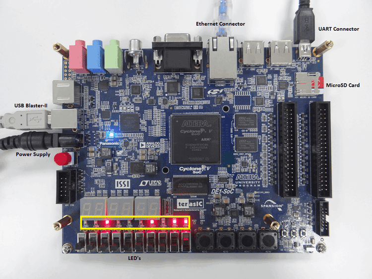
3. Ensure that you have properly installed the USB COM port device drivers on your computer.
4. Connect the UART and USB blaster port on the Terasic DE1-SoC to your computer.
5. Connect the Terasic DE1-SoC to your computer using an Ethernet cable. The default Terasic DE1-SoC IP address is 192.168.1.101.
6. Download the Terasic DE1-SoC Linux image file, extract the GZ archive, and then write the raw disc image file to the microSD card. Insert the microSD card in connector J11.
7. Set up the Intel Quartus tool path by using the hdlsetuptoolpath command:
hdlsetuptoolpath('ToolName', 'Altera Quartus II', 'ToolPath', quartuspath);Use your own Intel Quartus installation path when executing the command.
8. Set up the Terasic DE1-SoC hardware connection by using the following command:
h = alterasoc('192.168.1.101','root','cyclonevsoc');
Reference Design creation using Intel Quartus Prime
A reference design captures the complete structure of an SoC design, defining the different components and their interconnections. The HDL Coder SoC workflow generates an IP core that integrates with the reference design, and is then used to program an SoC board. The following figure describes the relationship between a reference design, an HDL IP core and an SoC board

In this section, we outline the basic steps necessary to create and export a simple reference design using the Intel Quartus and QSys environment. For more information about the QSys system integration tool, refer to Altera®/Intel documentation.
1. Create an empty Quartus project using the New project wizard with device part number as shown in the following figure

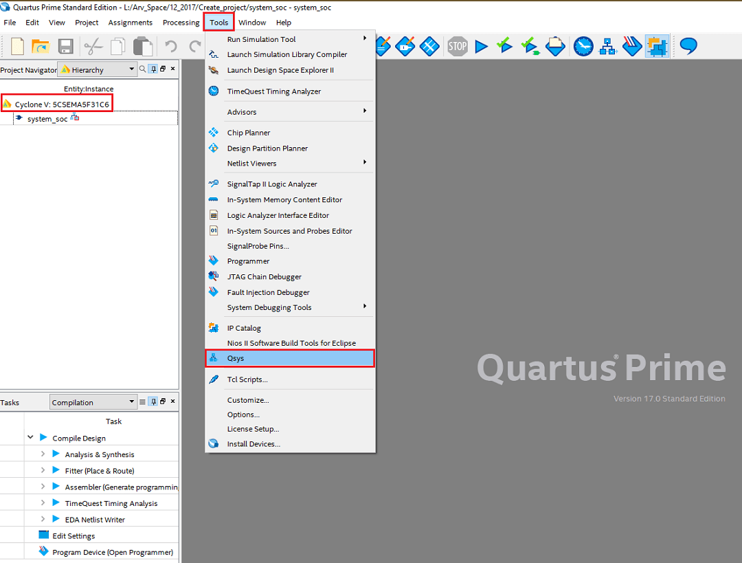
2. Initialize the Qsys in Quartus by navigating Tools --> Qsys as shown in the following figure
3. Select Cyclone-V Hard Processor System(HPS) & Altera PLL IP's from IP catalog to the created Qsys project. Enable HPS-to-FPGA user 0 clock (h2f_user0_clock) and connect that to refclk of Altera PLL as shown in the following figure
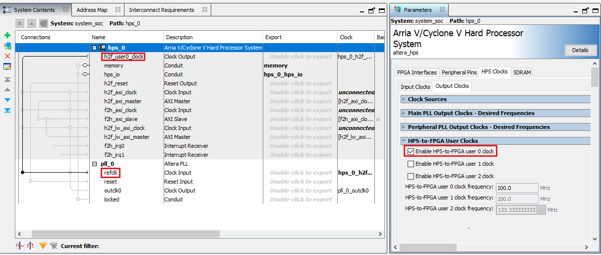
complete the other settings required for Hard Processor System such as Peripheral pin set and mode settings.
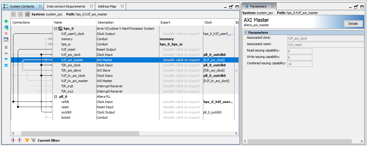
4. keep h2f_axi_master port connection open in order to connect to DUT IP during the process of workflow IP integration. Complete the rest of the connections between Altera PLL IP and HPS IP as shown in the following figure
5. Save the Qsys file. This file will be used while you create reference design plugin.
Register the DE1-SoC board in HDL Workflow Advisor
In this section, we outline the steps necessary to register the Terasic DE1-SoC development kit in HDL Workflow Advisor.
1. Create a board registration file with the name hdlcoder_board_customization.m and add it to the MATLAB® path.
A board registration file contains a list of board plug-ins. A board plugin is a MATLAB package folder containing a board definition file and all reference design plug-ins associated with the board.
The following code describes the contents of a board registration file that contains the board plugin DE1SoCRegistration to register the Terasic DE1-SoC development kit in HDL Workflow Advisor.
function r = hdlcoder_board_customization
% Board plugin registration file
% 1. Any registration file with this name on MATLAB path will be picked up
% 2. Registration file returns a cell array pointing to the location of
%    the board plugin
% 3. Board plugin must be a package folder accessible from MATLAB path,
%    and contains a board definition file
r = { ...
    'DE1SoCRegistration.plugin_board', ...
    };
end
2. Create the board definition file.
A board definition file contains information about the SoC board.
The following code describes the contents of the DE1-SoC board definition file plugin_board.m that resides inside the board plugin DE1SoCRegistration.
Information about the FPGA I/O pin locations ('FPGAPin') and standards ('IOSTANDARD') is obtained from the Pin Planner of Intel Quartus-II.
The property BoardName defines the name of the DE-1 SoC board as Terasic DE1-SoC development Kit in HDL Workflow Advisor.
function hB = plugin_board()
% Board definition
% Construct board object
hB = hdlcoder.Board;
hB.BoardName = 'Terasic DE1-SoC development Kit';
% FPGA device information
hB.FPGAVendor   = 'Altera';
hB.FPGAFamily   = 'Cyclone V';
hB.FPGADevice   = '5CSEMA5F31C6';
hB.FPGAPackage  = '';
hB.FPGASpeed    = '';
% Tool information
hB.SupportedTool = {'Altera QUARTUS II'};
% FPGA JTAG chain position
hB.JTAGChainPosition = 2;
%% Add interfaces
% Standard "External Port" interface
hB.addExternalPortInterface( ...
    'IOPadConstraint', {'IO_STANDARD "2.5V"'});
% Custom board external I/O interface
hB.addExternalIOInterface( ...
  'InterfaceID',    'LEDs General Purpose', ...
  'InterfaceType',  'OUT', ...
  'PortName',       'GPLED', ...
  'PortWidth',      10, ...
  'FPGAPin',        {'V16', 'W16', 'V17', 'V18', 'W17', 'W19', 'Y19', 'W20', 'W21', 'Y21'}, ...
  'IOPadConstraint', {'IO_STANDARD "3.3-V LVTTL"'});
hB.addExternalIOInterface( ...
   'InterfaceID',    'Switches', ...
   'InterfaceType',  'IN', ...
   'PortName',       'SW', ...
   'PortWidth',      10, ...
   'FPGAPin',        {'AB12', 'AC12', 'AF9', 'AF10','AD11', 'AD12', 'AE11', 'AC9', 'AD10', 'AE12'}, ...
   'IOPadConstraint', {'IO_STANDARD "3.3-V LVTTL"'});
hB.addExternalIOInterface( ...
   'InterfaceID',    'Push Buttons', ...
   'InterfaceType',  'IN', ...
   'PortName',       'KEY', ...
   'PortWidth',      4, ...
   'FPGAPin',        {'AA14', 'AA15', 'W15', 'Y16'}, ...
   'IOPadConstraint', {'IO_STANDARD "3.3-V LVTTL"'});
Register the custom reference design in HDL Workflow Advisor
In this section, we outline the steps necessary to register the custom reference design in HDL Workflow Advisor.
1. Create a reference design registration file named hdlcoder_ref_design_customization.m containing a list of reference design plugins associated with an SoC board.
A reference design plugin is a MATLAB package folder containing the reference design definition file and all files associated with the SoC design project. A reference design registration file must also contain the name of the associated board.
The following code describes the contents of a DE1-SoC reference design registration file containing the reference design plugin DE1SoCRegistration.qsys_base_170 associated with the board Terasic DE1-SoC development Kit.
function [rd, boardName] = hdlcoder_ref_design_customization
% Reference design plugin registration file
% 1. The registration file with this name inside of a board plugin folder
%    will be picked up
% 2. Any registration file with this name on MATLAB path will also be picked up
% 3. The registration file returns a cell array pointing to the location of
%    the reference design plugins
% 4. The registration file also returns its associated board name
% 5. Reference design plugin must be a package folder accessible from
%    MATLAB path, and contains a reference design definition file
rd = {'DE1SoCRegistration.qsys_base_170.plugin_rd', ...
     };
boardName = 'Terasic DE1-SoC development Kit';
end
2. Create the reference design definition file.
A reference design definition file defines the interfaces between the custom reference design and the HDL IP core that will be generated by the HDL Coder SoC workflow.
The following code describes the contents of the DE1-SoC reference design definition file plugin_rd.m associated with the board Terasic DE1-SoC development Kit that resides inside the reference design plugin DE1SoCRegistration.qsys_base_170. The property ReferenceDesignName defines the name of the reference design as Demo system in HDL Workflow Advisor.
function hRD = plugin_rd()
% Reference design definition
% Construct reference design object
hRD = hdlcoder.ReferenceDesign('SynthesisTool', 'Altera QUARTUS II');
hRD.ReferenceDesignName = 'Demo system';
hRD.BoardName = 'Terasic DE1-SoC development Kit';
% Tool information
hRD.SupportedToolVersion = {'17.0','17.1'};
%% Add custom design files
% add custom Qsys design
hRD.addCustomQsysDesign( ...
    'CustomQsysPrjFile', 'system_soc.qsys');
%% Add interfaces
% add clock interface
hRD.addClockInterface( ...
    'ClockConnection',     'pll_0.outclk0', ...
    'ResetConnection',     'hps_0.h2f_reset',...
    'DefaultFrequencyMHz', 50,...
    'MinFrequencyMHz',     5,...
    'MaxFrequencyMHz',     500,...
    'ClockModuleInstance', 'pll_0',...
    'ClockNumber',         0);
% add register interface
hRD.addRegisterInterface( ...
    'InterfaceConnection', 'hps_0.h2f_axi_master', ...
    'BaseAddress',         '0x0000');
The DE1-SoC reference design plugin folder DE1SoCRegistration.qsys_base_170 must contain the Qsys file system_soc.qsys saved previously from the Intel Quartus Prime project. The DE1-SoC reference design definition file plugin_rd.m identifies the SoC design project file via the following statement:
hRD.addCustomQsysDesign('CustomQsysPrjFile', 'system_soc.qsys');
In addition to the SoC design project files, plugin_rd.m also defines the interface connections between the custom reference design and the HDL IP core indicated in the following figure via the statements:
hRD.addClockInterface( ...
    'ClockConnection',     'pll_0.outclk0', ...
    'ResetConnection',     'hps_0.h2f_reset',...
    'DefaultFrequencyMHz', 50,...
    'MinFrequencyMHz',     5,...
    'MaxFrequencyMHz',     500,...
    'ClockModuleInstance', 'pll_0',...
    'ClockNumber',         0);
hRD.addRegisterInterface( ...
    'InterfaceConnection', 'hps_0.h2f_axi_master', ...
    'BaseAddress',         '0x0000');
Execute the SoC workflow for the Terasic DE1-SoC
The preceding sections discussed the steps to define and register the Terasic DE1-SoC and a custom reference design in the HDL Workflow Advisor for the SoC workflow. In this section, we use the custom board and reference design registration system to generate an HDL IP core that blinks LEDs on the Terasic DE1-SoC.
1. Add the Terasic DE1-SoC registration file to the MATLAB path using following commands.
example_root = (hdlcoder_intel_examples_root)
cd (example_root)
addpath(genpath('DE1SOC'));
2. Open the Simulink model that implements LED blinking using the command,
open_system('hdlcoder_led_blinking');

Generate an HDL IP core using the HDL Workflow Advisor
1. Using the IP Core Generation workflow in the HDL Workflow Advisor enables you to automatically generate a shareable and reusable IP core module from a Simulink model. HDL Coder generates HDL code from the Simulink blocks, and also generates HDL code for the AXI interface logic connecting the IP core to the embedded processor. HDL Coder packages all the generated files into an IP core folder. You can then integrate the generated IP core with a larger FPGA embedded design in the Intel Qsys environment.
2. Start the IP core generation workflow.
2.1. Open the HDL Workflow Advisor. Select the hdlcoder_led_blinking/led_counter subsystem. On the Apps tab, click HDL Coder. On the HDL Code tab, in the Assistance section, click Workflow Advisor.
2.2. In the Set Target > Set Target Device and Synthesis Tool task, for Target workflow, select IP Core Generation.
2.3. For Target platform, select Terasic DE1-SoC development Kit.
2.4. Click Run This Task to run the Set Target Device and Synthesis Tool task.
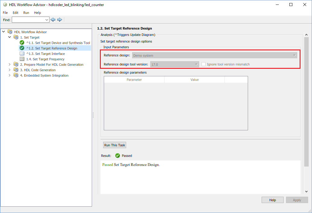
3. In the task 1.2, set target reference design default system is selected. click on Run This Task.
4. Configure the Target Interface.
Map each port in your DUT to one of the IP core target interfaces. In this example, input ports Blink_frequency and Blink_direction are mapped to AXI4. You can also select AXI4-lite as a target platform interface. The LED output port is mapped to an external interface, LEDs General Purpose [0:9], which connects to the LED hardware on the Terasic DE1-SoC development Kit.

5. Follow step 3 and step 4 of Generate an HDL IP core using the HDL Workflow Advisor section of Get Started with IP Core Generation for Intel SoC Devices example to generate IP core and view the IP core generation report.
6. Follow step 1 of Integrate the IP core with the Intel Qsys environment section of Get Started with IP Core Generation for Intel SoC Devices example to integrate the IP core in the reference design and create the Qsys project.
7. Now let us examine the Intel Qsys project created by the SoC workflow after completing the Create Project task under Embedded System Integration. The following figure shows the SoC project where we have highlighted the HDL IP Core. It is instructive to compare this project with the previous project used in the custom reference design plugin for a deeper understanding of the relationship between a custom reference design and an HDL IP Core.

8. Follow the steps 2, 3 and 4 of Integrate the IP core with the Intel Qsys environment section of Get Started with IP Core Generation for Intel SoC Devices example to generate software interface model, generate FPGA bitstream and program target device respectively.
9. The LEDs on the Terasic DE1-SoC will start blinking after loading the bitstream. In addition, you will be able to control the LED blink frequency and direction by executing the software interface model. Refer to Generate a software interface model section of Get Started with IP Core Generation for Intel SoC Devices example to control the LED blink frequency and direction from the generated software interface model.