High-Throughput Channelizer for FPGA
This example shows how to implement a high-throughput channelizer for hardware by using a polyphase filter bank.
The design uses vector input and parallel operations to achieve gigasamples-per-second (GSPS) data rates, also called super sample rates.
High speed signal processing is a requirement for applications such as radar, broadband wireless, and backhaul communication. Modern ADCs can sample signals at sample rates up to several GSPS, but the clock speeds for the fastest FPGA fall short of this sample rate. FPGAs typically run at hundreds of MHz. To perform GSPS processing on an FPGA, you can move from scalar processing to vector processing and process multiple samples in parallel at a much lower clock rate. Many modern FPGAs support the JESD204B standard interface, which accepts scalar input at a GHz clock rate and produces a vector of samples at a lower clock rate.
This example shows how to design a signal processing application that supports GSPS throughput. These Simulink® models assume that the input data is vectorized by using a JESD204B interface, and is available at a lower clock rate in the FPGA. The algorithm processes four samples at a time. Both models have a polyphase filter bank that consists of a filter and an FFT. The polyphase filter bank technique minimizes leakage and scalloping loss from the FFT. For more information about polyphase filter banks, see High Resolution Spectral Analysis in MATLAB (DSP System Toolbox).
The first part of the example uses the Channelizer (DSP HDL Toolbox) block from the DSP HDL Toolbox™ library, configured for a 12-tap filter. The Channelizer block uses the polyphase filter bank technique and automatically chooses data types, applies pipelining, and uses other optimizations for hardware performance and resource use. With this block, you can easily explore variations on your design.
The second part of the example implements a polyphase filter bank that has a 4-tap filter. This second part uses basic Simulink blocks. It shows the polyphase filter bank architecture, and the challenges of filter design for hardware, such as choosing data types and inserting pipeline stages.
Implement Channelizer with 12-Tap Filter
This model uses the Channelizer block, configured with a 12-tap filter, that results in good spectrum performance. Using the Channelizer block from the DSP HDL Toolbox library makes it easy to change design parameters such as coefficients, vector size, and FFT length. The block also automatically shares multipliers, calculates fixed-point data types, and pipelines the filter.
The model uses these workspace variables to configure the FFT and filter. The input vector size for this model is 4 samples. The model uses a 512-point FFT and a 12-tap filter for each band. The number of coefficients for the channelizer is 512 frequency bands times 12 taps per frequency band. Generate all the coefficients by using the tf(h) function.
simTime = 4000;
FFTLength = 512;
InVect = 4;
hc = dsp.Channelizer;
hc.NumTapsPerBand = 12;
hc.NumFrequencyBands = FFTLength;
hc.StopbandAttenuation = 60;
coef12Tap = tf(hc);
The input data consists of two sine waves, 200 kHz and 206.5 kHz. The frequencies are close to each other to illustrate the spectrum resolution of the channelizer.
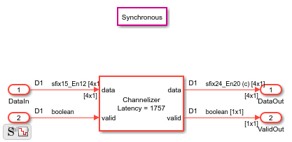
The Channelizer HDL Optimized subsystem contains the Channelizer block and a synchronous State Control block that generates hardware-optimized code for the enable logic within the channelizer.
The block implements pipeline stages around the multipliers so that the logic fits into FPGA DSP blocks, and implements the coefficient banks inside the channelizer with ROM blocks. These hardware-friendly options are the default behavior for the DSP HDL Toolbox blocks.
modelname = 'PolyphaseFilterBankHDLExample_HDLChannelizer';
open_system(modelname);
set_param(modelname,'SimulationCommand','Update');

This model diagram shows the Channelizer block inside the subsystem.
open_system([modelname,'/Channelizer HDL Optimized'])

The block has parameters to configure the filter coefficients, FFT length, and other settings that enable you to explore different hardware implementations of the algorithm.

View Simulation Results
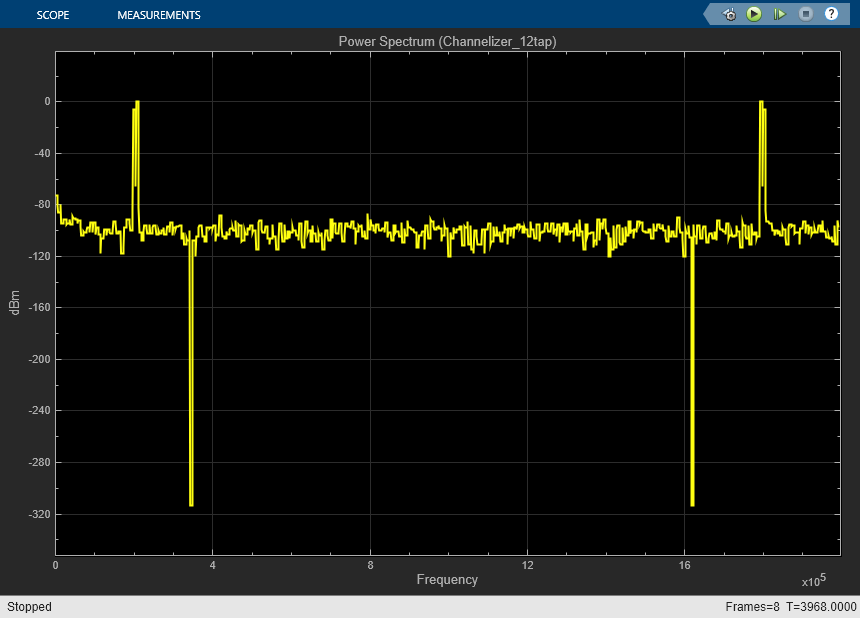
To visualize the spectrum result, open the spectrum viewer and run the model.
open_system([modelname,'/Spectrum Viewer/Power Spectrum viewer (Channelizer_12tap)']);
sim(modelname);

The spectrum viewer shows that the 12-tap filter separates the spectrum of the two signals. Zoom in between 100 kHz and 300 kHz to see where the channelizer detects two peaks. Two peaks is the expected result because the input signal has two frequency components.
Generate HDL Code
You must have the HDL Coder™ product to generate HDL code for this example model. Use this command to generate HDL code.
makehdl([modelname,'/Channelizer HDL Optimized']);
Use this command to generate a test bench that compares the results of an HDL simulation against the Simulink simulation behavior.
makehdltb([modelname,'/Channelizer HDL Optimized']);
The design was synthesized for AMD® Virtex 7 (xc7vx550t-ffg1158, speed grade 2). The design achieves a clock frequency of 361 MHz. At 4 samples per clock, this frequency results in 1.4 GSPS throughput.
The Minimize clock enable HDL code generation option is on in this model. The clock enable signal is a global signal, which is not recommended for high speed designs. In the model Configuration Parameters, choose HDL Code Generation, Global settings, Ports, and then select Minimize clock enable. This option is supported when the model is single rate.
The FFT block uses 56 DSP blocks on the FPGA, and the filter uses 48 DSP blocks.
 T = table(...
    categorical({'LUT'; 'LUT RAM'; 'FF'; 'BRAM'; 'DSP'}), ...
    [26641; 14585; 24816; 2; 104], ...
    'VariableNames',{'Resource','Usage'});

disp(T);
    Resource    Usage
    ________    _____

    LUT         26641
    LUT RAM     14585
    FF          24816
    BRAM            2
    DSP           104
Implement 4-Tap Polyphase Filter Bank
To show the internal implementation of a polyphase filter bank, the second example model implements a 512-point FFT by using the DSP HDL Toolbox FFT block and a 4-tap filter for each band by using basic Simulink blocks. The 4-tap filter has lower frequency resolution than the 12-tap filter in the first model, but it is easier to see the structure of the filter. These MATLAB® variables configure the blocks in the model. Use the dsp.Channelizer (DSP System Toolbox) System object™ to generate the coefficients. The polyphase method of the channelizer object generates a 512-by-4 matrix. Each row represents the coefficients for one band. Cast the coefficients to fixed-point types that have the same word length as the input signal.
h = dsp.Channelizer;
h.NumTapsPerBand = 4;
h.NumFrequencyBands = FFTLength;
h.StopbandAttenuation = 60;
coef4Tap = fi(polyphase(h),1,15,14,'RoundingMethod','Convergent');
The algorithm requires 512 filters (one filter for each band). For a vector input of 4 samples, the model implements four parallel 4-tap filters. Each filter applies 128 sets of coefficients.
ReuseFactor = FFTLength/InVect;
These variables configure the model to pipeline the multipliers and the coefficient bank to fit the logic into DSP blocks on the FPGA. Using the DSP blocks enables synthesis to a higher clock rate.
Multiplication_PipeLine = 2;
CoefBank_PipeLine       = 1;
The input data consists of two sine waves, 200 kHz and 250 kHz. These two frequencies are farther apart than the previous model because the smaller filter has lower spectrum performance. The input and output of the PolyPhaseFilterBank subsystem are 4-by-1 vectors.
modelname = 'PolyphaseFilterBankHDLExample_4tap';
open_system(modelname);
set_param(modelname,'SimulationCommand','Update');

The PolyphaseFilterBank subsystem contains the Coefficient Bank subsystem that rotates over the coefficient sets. The Filter Bank subsystem accepts vectors of coefficients and data and returns a vector of filtered data. The FFT block also accepts and returns a vector of 4 samples, and implements a hardware-optimized architecture.
open_system([modelname,'/PolyPhaseFilterBank'])

This model diagram shows the pipelined 4-tap filter implementation.
open_system([modelname,'/PolyPhaseFilterBank/Filter Bank'])

View Simulation Results
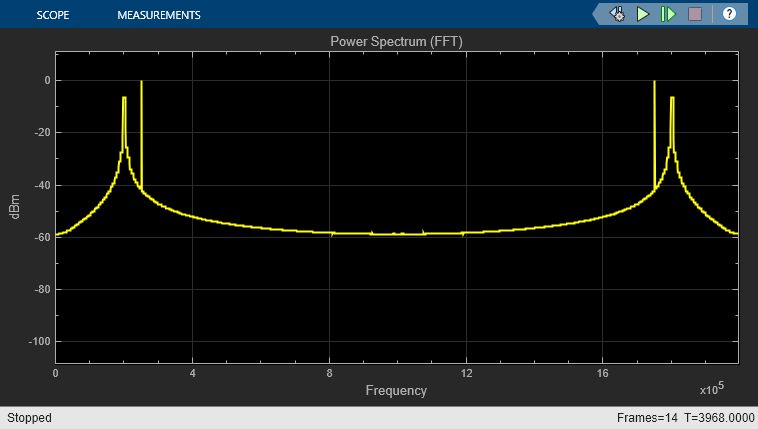
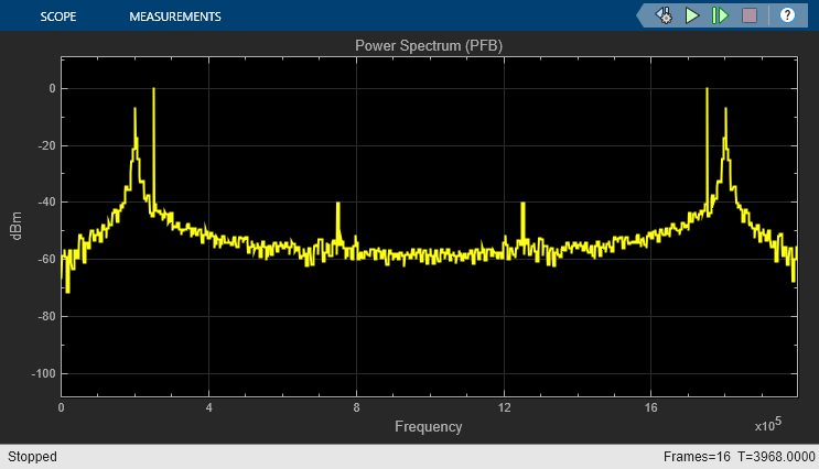
To visualize the result of the simulation, open the spectrum viewers and run the model.
open_system([modelname,'/FFT Spectrum Viewer/Power Spectrum viewer (FFT)']);
open_system([modelname,'/PFB Spectrum Viewer/Power Spectrum viewer (PFB)']);
sim(modelname);


The polyphase filter bank spectrum viewer shows the improvement in the power spectrum and minimization of frequency leakage and scalloping compared with using only an FFT. By comparing the two spectrums, and zooming in between 100 kHz and 300 kHz, you can see that the polyphase filter bank has fewer peaks over –40 dB than the classic FFT.
Considerations for Optimized Hardware
Data Type
Data word length affects both the accuracy of the result and the resources used in the hardware. This 4-tap filter uses full precision. With an input data type of fixdt(1,15,13), the output is fixdt(1,18,17). The absolute values of the filter coefficients are all smaller than 1, so the data does not grow after each multiplication operation. Each addition adds one bit to the data type. To keep the accuracy in the FFT, the data type grows one bit for each stage. This growth makes the twiddle factor multiplication larger at each stage. For many FPGAs, a multiplication size smaller than 18-by-18 is desirable. Because a 512-point FFT has 9 stages, the input of the FFT cannot be more than 11 bits. The first 8 binary digits of the maximum coefficient in this case are zero. Therefore, this example casts the coefficients to fixdt(1,7,14) instead of fixdt(1,15,14). Also, the maximum value of the Datatype block output inside the polyphase filter bank has 7 leading zeros after the binary point, so the model casts the filter output to fixdt(1,11,17). These adjustments keep the FFT internal multiplier size smaller than 18-by-18 and save hardware resources.
Design for Speed
The model uses these settings to enable the generated HDL code to synthesize to a faster clock rate.
Synchronous State Control block — Implements hardware-friendly enable logic for Delay blocks.
Minimize clock enable — Avoids implementing a global clock enable signal that could decrease the synthesized clock rate.
Use DSP block in FPGA — Maps multipliers into DSP blocks in the FPGA by including 2 delays before each multiplier and 2 delays after. These pipeline registers cannot have a reset signal. Set the reset type to none for each pipeline by right-clicking the Delay block and in the HDL Coder app section, click HDL Block Properties, then setting Reset Type to
None.Use ROM in FPGA — Map the combinatorial logic inside the Coefficient MATLAB Function block (inside the
Coefficient Banksubsystem) to a ROM by adding a register after the block. The delay length is set byCoefBank_PipeLine. Set the reset type for these delays to none.
Generate HDL Code
You must have the HDL Coder™ product to generate HDL code for this example model. Use this command to generate HDL code.
makehdl([modelname,'PolyPhaseFilterBank']);
Use this command to generate a test bench that compares the results of an HDL simulation against the Simulink simulation behavior.
makehdltb([modelname,'PolyPhaseFilterBank']);
When the design is synthesized for AMD® Virtex 7 (xc7vx550t-ffg1158, speed grade 2), the design achieves a clock frequency of 324 MHz (before place and route). At 4 samples per clock, this frequency results in 1.3 GSPS throughput.
The FFT block uses 56 DSP blocks in the FPGA, and the filter uses 16 DSP blocks.
 T = table(...
    categorical({'LUT'; 'LUT RAM'; 'FF'; 'BRAM'; 'DSP'}), ...
    [14713; 3570; 21514; 2; 72], ...
    'VariableNames',{'Resource','Usage'});

disp(T);
    Resource    Usage
    ________    _____

    LUT         14713
    LUT RAM      3570
    FF          21514
    BRAM            2
    DSP            72
Conclusion
The first part of the example shows how the Channelizer block from the DSP HDL Toolbox library makes it easy to implement an algorithm for hardware, and provides quick exploration of design options.
The second part of the example shows design considerations when implementing filters for hardware without using a hardware-optimized library block, such as choosing data types and inserting pipeline stages. When you use the library blocks from DSP HDL Toolbox, you do not have to consider these factors yourself. The blocks implement hardware-optimized algorithms that are ready for HDL code generation and deployment to FPGAs or ASICs.