Data Capture Workflow
Use FPGA data capture to observe signals from your design while the design is running on the FPGA. The FPGA data capture feature captures a window of signal data from the FPGA and returns the data to MATLAB® or Simulink® over a JTAG, Ethernet, or USB Ethernet interface.
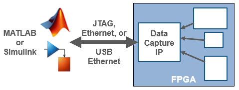
FPGA data capture over a JTAG connection is available for Intel® and AMD® devices. FPGA data capture over an Ethernet or USB Ethernet connection is available for AMD devices only. For a complete list of supported devices and interfaces, see Supported FPGA Devices for FPGA Verification.
HDL Coder and Existing HDL Design Workflows
You can use one of two workflows to capture data from your FPGA or SoC device and send it to MATLAB or Simulink:
HDL Coder™ Workflow — When you generate the HDL IP with HDL Coder, use the HDL Workflow Advisor tool to generate the data capture IP and integrate it in the design. For an example, see Debug IP Core Using FPGA Data Capture (HDL Coder).
Existing HDL Design Workflow — If you have an existing HDL design, use HDL Verifier™ tool to generate the data capture IP. Then, integrate the generated IP into your FPGA design. For an example, see Capture Temperature Sensor Data from AMD FPGA Board Using FPGA Data Capture or Capture Audio Signal from Intel FPGA Board Using FPGA Data Capture.
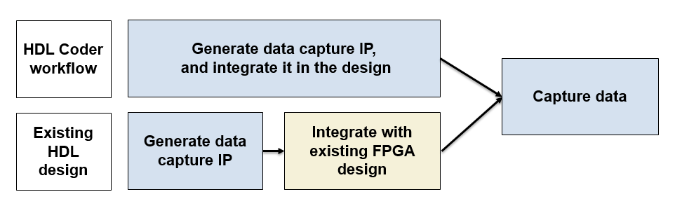
In both workflows, to capture signals from your design, HDL Verifier generates an IP core that communicates with MATLAB. Use the HDL Coder workflow to automatically integrate the data capture IP core in your design. Otherwise, manually integrate this IP core into your HDL project and deploy it to the FPGA along with the rest of your design. Then, use one of the following methods to capture data.
Capture data and send it to MATLAB — HDL Verifier generates a customized tool that returns the captured signal data. Alternatively, you can use the generated System object™ to capture data programmatically.
Capture data and send it to Simulink — HDL Verifier generates a block that has output ports corresponding to the signals you captured.
Key Data Capture Capabilities
At generation time, you can specify the number of data capture IPs to generate the storage type for captured data, and whether to include trigger input and output ports in the generated data capture IPs. At run-time, you can specify data types for the captured data, the number of windows to capture, trigger conditions that control when to capture the data, and a capture condition that controls which data to capture.
Multiple Data Capture IPs — For an AMD device over a JTAG connection, you can observe signals operating at different clock rates by using multiple data capture IPs. For more information about how to generate and integrate multiple data capture IPs into your FPGA design, see Capture Asynchronous Data.
Note
Support for multiple data capture IPs is available only when you follow the existing HDL design workflow.
Cross-Trigger — For an AMD device over a JTAG connection, you can specify whether to include trigger input and output ports to each data capture IP. Include trigger input and output ports to enable cross-triggering between multiple data capture IPs and between a data capture IP and a processor. Use these ports to pass the trigger signal from one data capture IP to another.
External Memory — You can configure the memory type for storing captured data as either internal memory or external memory. Internal memory uses internal BRAM resources to store captured data, while external memory uses external DDR memory connected to the FPGA for storage. You can capture large data sets up to two gigasamples by utilizing the external DDR memory connected to the FPGA for an AMD device.
Trigger Condition — When the design is running on the FPGA, first the generated IP core waits for the trigger condition. Define a trigger condition that initiates when the values of one or more signals match the specified criteria. When the IP core detects the trigger, the logic captures the designated signals in a buffer and returns the data over the JTAG, Ethernet, or USB Ethernet interface to the host machine. You can then analyze and display these signals in your MATLAB workspace or Simulink model. For more information about trigger condition, see Triggers.
Sequential Trigger — You can provide a sequence of trigger conditions at multiple stages to capture specified data from an FPGA. With a sequential trigger, you can read data to MATLAB or Simulink only after all of the specified trigger conditions happen in sequence. For more information about sequential trigger, see Sequential Trigger.
Capture Condition — To make the best use of the buffer size and capture only the valid data, you can also define a capture condition. Define a capture condition in the same way as you define the trigger condition. When both the conditions are satisfied, the logic captures only the valid values of the designated signals. For more information about capture condition, see Capture Conditions.
Generate and Integrate Data Capture IP Core Using HDL Coder Workflow
In this workflow, when you use the HDL Workflow Advisor tool to generate your HDL design, first mark interesting signals as test points in Simulink. Configure your design using the HDL Workflow Advisor tool to:
Select the type of connection channel by setting the FPGA Data Capture (HDL Verifier required) parameter in the Set Target Reference Design task. For more information, see Set Target Reference Design (HDL Coder).
Enable test point generation by selecting the Enable HDL DUT port generation for test points parameter in the Set Target Interface task. For more information, see Set Target Interface (HDL Coder).
Connect test point signals to the
FPGA Data Captureinterface in the Set Target Interface task.Set up storage type, buffer size, and maximum sequence depth for data collection in the Generate RTL Code and IP Core task. To include capture condition logic in the IP core, select Include capture condition logic in FPGA Data Capture. For more information, see Generate RTL Code and IP Core (HDL Coder).
Then, run through the remaining steps to generate HDL code for your design and program the FPGA. The data capture IP core is integrated in the generated design. In this case, the data capture IP operates on a single-clock rate, which is the primary clock of your device under test (DUT). You are now ready to Capture Data.
Generate Data Capture IP Core Using Existing HDL Design Workflow
In this workflow, before you can capture FPGA data, first specify which signals to capture and how many samples to return. Use the FPGA Data Capture Component Generator tool to configure these and other settings and to generate the HDL IP core. The IP core contains:
A port for each signal you want to capture or use as part of a trigger condition
Memory to capture the number of samples you requested for each signal
JTAG, Ethernet, or USB Ethernet interface logic to communicate with MATLAB
Trigger and capture condition logic that you can configure at run time
A ready-to-capture signal to control data flow from the FPGA

The tool also generates a customized FPGA Data Capture tool, System object, and model that communicate with the FPGA.
Integrate IP Core into FPGA Using Existing HDL Design Workflow
For MATLAB to communicate with the FPGA, you must integrate the generated HDL IP core into your FPGA design. Follow the instructions in the generation report based on your device family.
Intel Devices
Follow these instructions to integrate the datacapture HDL IP core into
your FPGA design that targets an Intel device.
Create a Quartus® project.
Navigate to the
hdlsrcfolder.Add the generated HDL files in the
hdlsrcfolder to your Quartus project. Then, instantiate the HDL IP core,datacapture, in your HDL code. Connectdatacaptureto the signals selected for data capture and specifying the triggers.Compile the project and program the FPGA with the new image through a JTAG connection.
AMD Non-Versal Devices
Follow these instructions to integrate the data capture HDL IP core into your FPGA design that targets an AMD non-Versal® device.
Create a Vivado® project.
In the Vivado Tcl console, navigate to the destination folder that contains the generated data capture IP, for example,
hdlsrc.Follow one of these steps based on your connection type.
JTAG
Follow these instructions if you set Connection type to
JTAGin the FPGA Data Capture Component Generator tool.Insert the data capture IP along with the JTAG Debug Hub IP into your block design, and establish the required connections by executing this command in the Vivado Tcl console. The JTAG Debug Hub IP communicates with MATLAB on the host machine and with the data capture IP in the FPGA design.
source ./insertFPGADataCaptureIP.tcl
This Tcl script connects the BSCAN subordinate (BSCAN_S) and
dc_activeports of the data capture IP to the BSCAN manager (BSCAN_M1) andactive_s1ports of the JTAG Debug Hub IP, respectively. The JTAG Debug Hub IP controls the data capture IP through this active signal.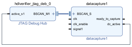
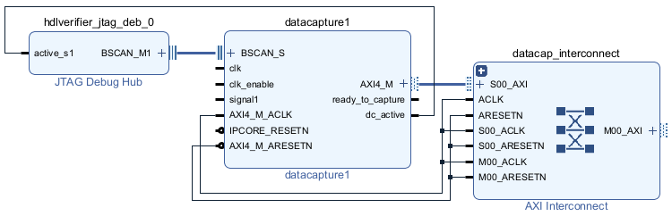
Additionally, for the external memory storage type, this Tcl script inserts an AXI Interconnect IP into the block design and connects the AXI4 manager (AXI4_M) interface of the data capture IP to the AXI4 subordinate (S00_AXI) interface of the AXI Interconnect IP.
Alternatively, you can add the generated data capture IP and the JTAG Debug Hub IP from a specified folder to the user repository of your Vivado project by using the
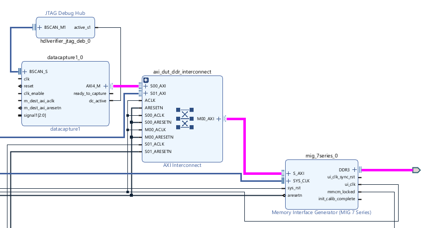
addFPGADataCaptureToVivadofunction. Then, manually insert and connect these IPs into your block design.External memory only — Connect the AXI4 manager (M00_AXI) interface of the AXI Interconnect IP to the AXI4 subordinate (S_AXI) interface of MIG, as this figure shows.
PL Ethernet
Follow these instructions if you set Connection type to
PL Ethernetin the FPGA Data Capture Component Generator tool.Insert the data capture IP along with the Ethernet MAC Hub IP into your block design, and establish the required connections by executing this command in the Vivado Tcl console. The Ethernet MAC Hub IP communicates with MATLAB on the host machine and with the data capture IP in the FPGA design.
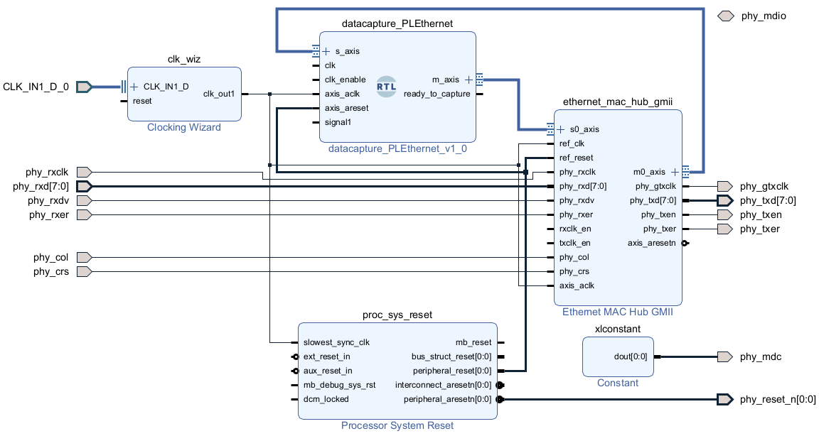
This Tcl script connects the data capture IP to the Ethernet MAC Hub IP, as this figure shows.source ./insertFPGADataCaptureIP.tcl
Additionally, for the external memory storage type, this Tcl script inserts an AXI Interconnect IP into the block design and connects the AXI4 manager (AXI4_M) interface of the data capture IP to the AXI4 subordinate (S00_AXI) interface of the AXI Interconnect IP.
External memory only — Connect the AXI4 manager (M00_AXI) interface of the AXI Interconnect IP to the AXI4 subordinate (S_AXI) interface of MIG, as this figure shows.

PS Ethernet or USB Ethernet
Follow these instructions if you set Connection type to
PS EthernetorUSB Ethernetin the FPGA Data Capture Component Generator tool.Note
For PS Ethernet and USB Ethernet interfaces, you must set up the target SoC device and the host computer before you perform the data capture operations. For more information, see Capture Data over PS Ethernet for PS Ethernet and Capture Data over USB Ethernet for USB Ethernet.
Insert the data capture IP into your block design by executing this command in the Vivado Tcl console.
source ./insertFPGADataCaptureIP.tcl
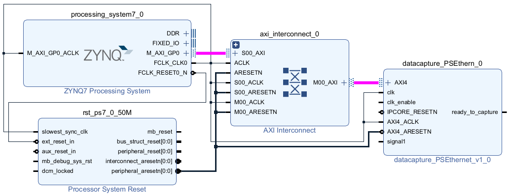
Connect the subordinate AXI4 interface of the data capture IP to the manager AXI4 interface of the processor.
External memory only — Connect the AXI4 manager (AXI4_M) interface of the data capture IP to the AXI4 subordinate (S_AXI) interface of MIG through AXI Interconnect, as this figure shows.

Connect data capture IP to the signals selected for data capture and specifying the triggers.
Complete the block design by connecting the clock, clock enable, and reset signals.
JTAG only — Complete the block design by connecting the
clkandclk_enableinput ports of the data capture IP. Additionally, for external memory, connect theAXI4_M_ACLK,AXI4_M_ARESETN, andIPCORE_RESETNinput ports of the data capture IP.PL Ethernet only — Complete the block design by connecting the
clkclk_enable,axis_aclk, andaxis_aresetinput ports of the data capture IP. Additionally, for external memory, connect theAXI4_M_ACLK,AXI4_M_ARESETN, andIPCORE_RESETNinput ports of the data capture IP.PS Ethernet or USB Ethernet only — Complete the block design by connecting the
clk,clk_enable,IPCORE_RESETN,AXI4_ACLK, andAXI4_ARESETNinput ports of the data capture IP. Additionally, for external memory, connect theAXI4_M_ACLKandAXI4_M_ARESETNinput ports of the data capture IP.External memory only — Make sure that the
AXI4_M_ACLK, used by the data capture IP to write data to external DDR memory, has a higher frequency than theclkclock.JTAG or PL Ethernet only — Compile the project and program the FPGA with the new image through a JTAG or Ethernet connection.
PS Ethernet or USB Ethernet only — Use the
loadBitstreamfunction to load the BIT and DTB files based on your FPGA design. For the steps to generate a device tree blob (DTB) file, follow the instructions in the generation report. For more information about DTB file generation steps, see Generate DTB File.
AMD Versal Devices
Follow these instructions to integrate the data capture HDL IP core into your FPGA design targeted on an AMD Versal device.
Note
FPGA data capture support for Versal devices is available for JTAG connections only.
Create a Vivado project.
In the Vivado Tcl console, navigate to the destination folder that contains the generated data capture IP, for example,
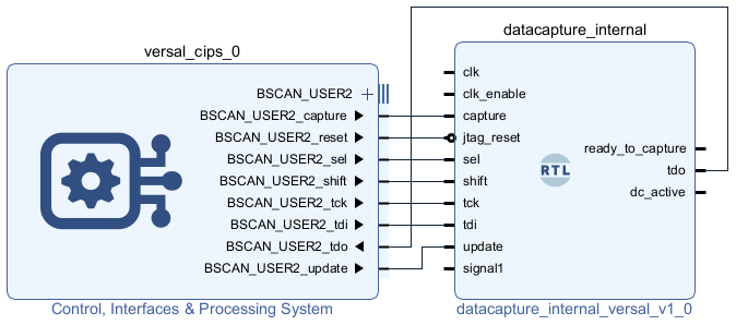
hdlsrc.Insert the data capture IP into your block design and connect the IP to the BSCAN_USER2 interface of the AMD Versal platform CIPS IP by executing this command in the Vivado Tcl console.
To enable the BSCAN_USER2 interface, enable the PL BSCAN1 interface in the CIPS IP.source ./insertVersalFPGADataCaptureIP.tcl
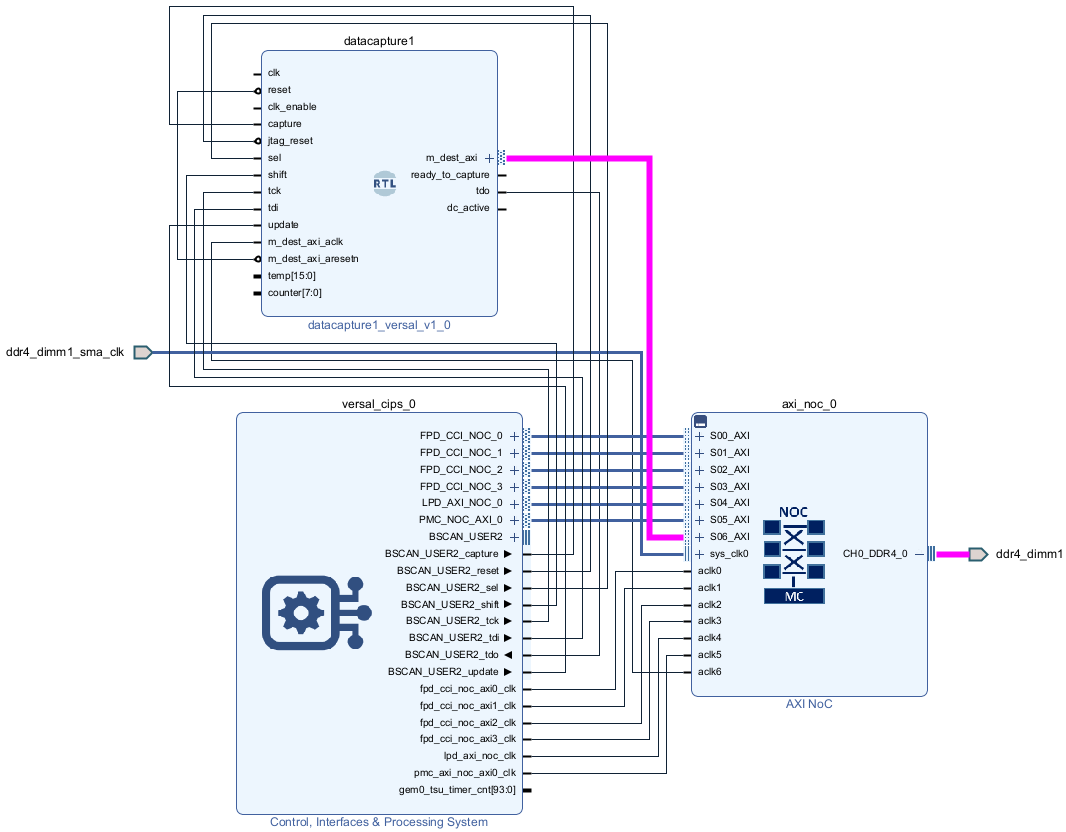
External memory only — Connect the AXI4 manager (m_dest_axi) interface of the data capture IP to the AXI4 subordinate (S_AXI) interface of the AMD AXI NoC IP, as this figure shows.
Connect data capture IP to the signals selected for data capture and specifying the triggers.
Complete the block design by connecting the
clkandclk_enableinput ports of the data capture IP. Additionally, for external memory, connect theAXI4_M_ACLK,AXI4_M_ARESETN, andIPCORE_RESETNinput ports of the data capture IP.External memory only — Make sure that the
AXI4_M_ACLK, used by the data capture IP to write data to external DDR memory, has a higher frequency than theclkclock.Compile the project and program the FPGA with the new image through a JTAG cable.
Capture Data
The FPGA data capture IP core communicates over the JTAG, Ethernet, or USB cable between your FPGA board and the host computer. Make sure that the required cable is connected. Before capturing data, you can set data types for the captured data, set a trigger condition that specifies when to capture the data, and set a capture condition that specifies the data to be captured. To configure these options and capture data, you can:
Open the FPGA Data Capture tool. Set the trigger, capture condition, and data type parameters, and then capture data into the MATLAB workspace.
Use the generated System object derived from
hdlverifier.FPGADataReader. Set the data types, trigger condition, and capture condition using the methods and properties of the System object, and then call the object to capture data.In Simulink, open the generated model and configure the parameters of the FPGA Data Reader block. Then run the model to capture data.
Set Base Address of External DDR Memory (for JTAG, PS Ethernet, and USB Ethernet with External Memory Only)
For JTAG, PS Ethernet, and USB Ethernet connections with external memory, set the base
address of the external DDR memory. To do this, use the MemoryBaseAddress
property of the hdlverifier.FPGADataReader
System object before capturing data to MATLAB. Set the External DDR memory base
address parameter of the FPGA Data Reader block before capturing
data to Simulink.
For example, the following command sets the base address of the DDR memory for the
datacapture1
System object to 80000000.
datacapture1.MemoryBaseAddress = "80000000";Set Base Address of Data Capture IP and IP Address of Target Device (for PS Ethernet and USB Ethernet Only)
For PS Ethernet and USB Ethernet connections, set the base address of the data capture IP
and the IP address of the target device. To do this, use the CaptureBaseAddress
and DeviceAddress
properties of the hdlverifier.FPGADataReader
System object before capturing data to MATLAB. Set the Device IP address
and Data Capture IP core base
address parameters of the FPGA Data Reader block before capturing
data to Simulink.
For example, the following commands set the base address of the
datacapture1 data capture IP to 40000000 and the IP
address of the target device to 192.168.5.2.
datacapture1.CaptureBaseAddress = "40000000";
datacapture1.DeviceAddress = "192.168.5.2";
Export Data Capture Settings to MATLAB Script
You can optionally export the current data capture settings such as number of capture windows, number of trigger stages, trigger position, trigger and capture condition settings, and data type settings to a MATLAB script by using the Export Settings button in the FPGA Data Capture tool.
The exported MATLAB script provides a programmable interface to customize and automate the data capture process. You can bypass repetitive UI interactions by editing and reusing the exported script for iterative data capture.
To capture data by using the exported script, follow one of these options:
Import the data capture settings from the script into the FPGA Data Capture tool.
The
launchAppfunction in the script opens the tool with the configured data capture settings. Then, capture data from the tool.Edit the script to call the data capture object.
If you do not want to import the data capture settings into the FPGA Data Capture tool, comment out this command in the script.
fpgadc_obj.launchApp
Call the data capture object directly or use the
stepfunction.For example, the following command calls the
fpgadc_objdata capture object to capture data.[Capture_Window,Trigger_Position,dataOut] = fpgadc_obj();
After you capture the data and import it into the MATLAB workspace or Simulink model, you can analyze, verify, and display the data.
See Also
FPGA Data
Capture Component Generator | FPGA Data
Capture | hdlverifier.FPGADataReader | FPGA Data
Reader