Pulse-Doppler Radar Using AMD RFSoC Device
This example shows how to build, simulate, and deploy a pulse-Doppler radar system in Simulink® using an SoC Blockset™ implementation targeted on the AMD® Zynq® UltraScale+™ RFSoC evaluation kits. Using this example, you can detect and estimate the range and velocity of moving targets. The range-Doppler processing is partitioned across a field-programmable gate array (FPGA) and a processor. The range processing is handled in the FPGA and the Doppler processing is handled in the processor. The example also implements a radar target emulator to evaluate the performance of the radar.
Supported Hardware Platforms
AMD Zynq UltraScale+ RFSoC ZCU111 evaluation kit + XM500 balun card
AMD Zynq UltraScale+ RFSoC ZCU216 evaluation kit + XM655 balun card
AMD Zynq UltraScale+ RFSoC ZCU208 evaluation kit + XM655 balun card
AMD Zynq UltraScale+ RFSoC DFE ZCU670 evaluation kit + XM755 balun card
Design Task
Target detection is an important part of a radar system. Range and Doppler estimation improve the detection capabilities. In this example a pulsed radar detects the velocity of the moving targets at specific ranges. The velocity is derived from the Doppler shift caused by the moving targets. The pulsed radar identifies the existence of a target at a given range and then uses Doppler processing to determine the radial velocity of the target at that range. You can visualize a signal in the range-Doppler domain to identify connections among the targets. For more information, see Range-Doppler Response (Phased Array System Toolbox) of pulsed-radar systems. To view a range-response map, see the phased.RangeDopplerScope (Phased Array System Toolbox) System object.
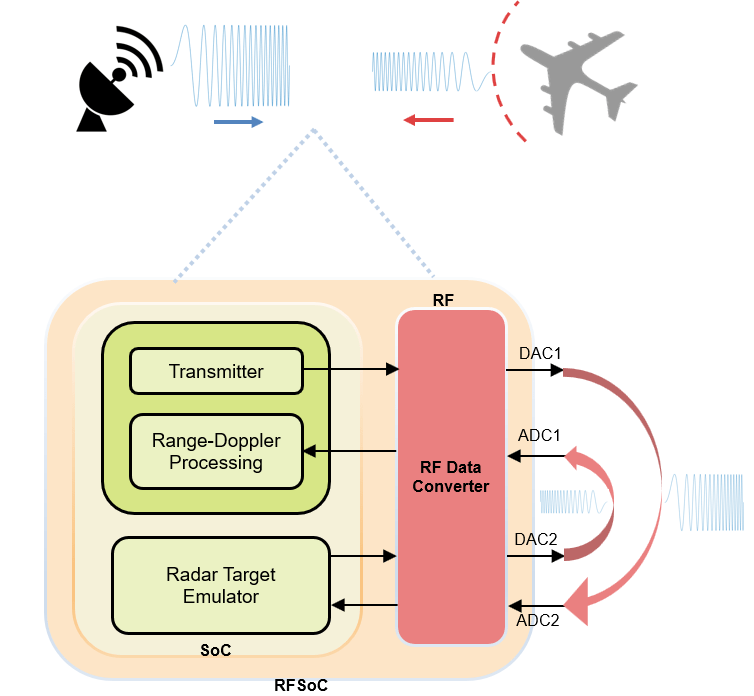
In this example, the design task is to model the complete range-Doppler processing system consisting of a transmitter, a receiver, and a radar target emulator in Simulink and to implement the system on an RFSoC device.
The transmitter in the range-Doppler processing generates a linear FM (LFM) pulse and transmits through one DAC channel. The target emulator receives the radar waveform, modifies the signals to emulate one or more targets at a given range and velocity, and retransmits the signal. The receiver receives the target emulated signals and applies the range and Doppler processing to extract the range and velocity information. In this example, the range is extracted using a Matched filter and the velocity using an FFT.
System Specifications
The following are the system specifications:
Radar signal bandwidth at Ka-band = 200 MHz
Maximum range per pulse interval = 700 m
Maximum range resolution <= 1 m
Maximum unambiguous velocity >= 300 m/s
Velocity resolution <= 10 m/s
The following figure shows the implementation block diagram of the pulse-Doppler radar system.

Design Using SoC Blockset
This example contains four different top models.
soc_range_doppler_zcu111_toprange doppler processing on zcu111 evaluation kit.soc_range_doppler_zcu216_toprange doppler processing on zcu216 evaluation kit.soc_range_doppler_zcu208_toprange doppler processing on zcu208 evaluation kit.soc_range_doppler_zcu670_toprange doppler processing on zcu670 evaluation kit.
This example shows the workflow using the soc_range_doppler_zcu111_top model. The workflow steps are common for all the four models.
Create the SoC model soc_range_doppler_zcu111_top as the top model and set the hardware board to the AMD Zynq UltraScale+ RFSoC ZCU111 evaluation kit. This model includes FPGA model soc_range_doppler_fpga and processor model soc_range_doppler_proc, which are instantiated as model references. The top model also includes AXI4-Stream to Software block that share the external memory between the FPGA and the processor.
open_system('soc_range_doppler_zcu111_top')

close_system('soc_range_doppler_zcu111_top')
RF Data Converter Configuration
RFSoC devices have an RF Data Converter hardware IP connected to the programmable logic, which needs to be configured as per the application requirements. SoC Blockset provides an RF Data Converter (RFDC) block in Simulink, which provides an interface to the AMD RF Data Converter IP. This block enables you to configure the ADC and DAC settings of the AMD RF Data Converter IP and emulates the programmable logic interface to the converters.
To meet the system requirements of a 200 MHz radar signal bandwidth, design and set the RF Data Converter block configuration by following these steps.
1. Choose the decimation factor and ADC sample rate based on the signal bandwidth.
The pass band for decimation filters must be 80 percent of Nyquist. To meet this passband requirement, use this condition. (0.8 x Fs / D)
 signal bandwidth
To meet the signal bandwidth of 200 MHz, choose the decimation factor (D) as 8. To calculate the ADC sample rate (Fs), use this equation. Fs
 (signal bandwidth x D /0.8) = (200 x 8/0.8) = 2000 MHz.
2. Choose 2 samples per clock so that the FPGA clock rate is 125 MHz. The FPGA clock rate is calculated by Fs /(D x samples per clock) = 2000/(8 x 2) = 125 MHz.
3. Choose the receiver intermediate frequency (IF) as 500 MHz.
Configure the RF Data Converter block according to these values. Set the NCO frequency for the DAC and ADC mixers to 0.5 GHz and the ADC and DAC sample rates to 2000 MSPS. You must set the values of the Interpolation mode (xN), Decimation mode (xN), and Samples per clock cycle parameters such that the effective clock rate for the FPGA algorithm is the desirable value for this example, which is 125 MHz. This value is calculated and displayed on the block mask as the Stream clock frequency (MHz) parameter after you click Apply. Set the Decimation mode (xN) parameter to 8, so that the effective sample rate after decimation is 250 MSPS. To get a clock rate of 125 MHz, in the DAC tab, set the Samples per clock cycle parameter to 2. Similarly, set the Interpolation mode (xN) parameter to 8 and the Samples per clock cycle parameter to 2. These settings imply that the Stream clock frequency is 2000/(8 x 2) = 125 MHz.
The ZCU111 evaluation board comes with an XM500 eight-channel loopback card. This card has two ADC and two DAC single-ended channels (ADC224_T0_CH0, ADC224_T0_CH1, DAC229_T1_CH2, and DAC229_T1_CH3) for supporting the selected IF frequency of 500 MHz. Set the RF interface parameter to Customize. Then, select these specific channels: ADC 0 and ADC 1 in Tile 0 in the ADC tab and DAC 2 and DAC 3 in Tile 1 in the DAC tab as shown in the following figure.

Hardware Logic Design
The FPGA model soc_range_doppler_fpga contains two subsystems: Range Doppler Tx-Rx and Radar Target Emulator. The Radar Target Emulator subsystem acts as a real target.
open_system('soc_range_doppler_fpga')

close_system('soc_range_doppler_fpga')
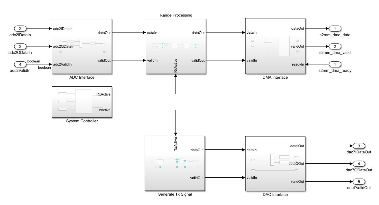
In the Range Doppler Tx-Rx subsystem, the Generate TX Signal block generates the pulsed LFM signal and transmits the signal through the DAC 2 in Tile 1 interface in the transmit path. In the receive path, the ADC Interface block receives the samples and performs the matched filtering for range processing, followed by Hamming windowing as the first step in Doppler processing. The DMA Interface sends the estimated range bins to the processor for the remaining Doppler processing through the memory. The System Controller block synchronizes the radar transmit and receive processes.

The Radar Target Emulator subsystem receives the emulator configuration from the processor through AXI4-Lite registers. This subsystem receives the transmitted signal through the ADC 0 in Tile 0 interface and emulates the range delay, Doppler shift, and free space path loss of the targets based on the configuration that you have set. This emulated target data is retransmitted through the DAC 3 in Tile 1 interface as the reflected signal from the target.
Processor Logic Design
The software functionality is partitioned across four tasks with characteristics that you can configure using the Task Manager block.
1. baseRateTask
Type of task: Timer
Task period: 0.2 s
Function: Control the timing execution of the software.
2. dataReadTask
Type of task: Event-based task
Function: Receive the range bins processed from the FPGA through the Stream Read block, and then send those bins for FFT-based Doppler processing. The UDP Write block sends the final computed range-Doppler response to the host. The
DMAReadFcnsubsystem holds the functionality of this task.
3. udpRxTask
Type of task: Event-based task
Function: Receive configuration information from the host through the user datagram protocol (UDP) interface. The UDP packet handler parses the packet to get the configuration information and applies it to the radar system controller in the FPGA through the AXI4-Lite registers. It also passes the radar target emulator configuration to the RadarTargetUpdate task. The
UDPRxFcnsubsystem holds the functionality of this task.
4. radarTargetUpdateTask
Type of task: Timer
Task period: 0.01 s
Function: Configure and update the target emulator registers in the FPGA through the AXI4-Lite interface. The function uses the target emulator information, such as radar cross section (RCS), range, velocity and the enable from the udpRxTask, to configure the target emulator. The
RadarTargetUpdateFcnsubsystem holds the functionality of this task.
open_system('soc_range_doppler_proc')

close_system('soc_range_doppler_proc')
Simulate
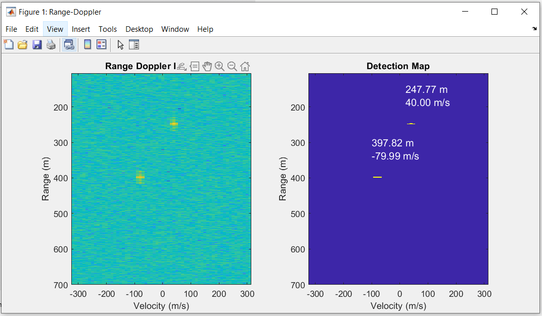
To confirm the basic operation, run the model and observe the estimated range and velocity of the moving targets on the Range Doppler Response and Detection Map plot. The Range Doppler Response displays the power level for each range and velocity bin. The Detection Map shows the result of 2-D constant false alarm rate (CFAR) detection and density-based spatial clustering of applications with noise (DBSCAN) clustering on the range-Doppler response to extract the distinct targets and their estimated range and velocity. This detection processing is done on the host machine in MATLAB®.

Implement and Run on zcu111 Hardware
Hardware Setup
Connect the SMA connectors on the XM500 Balun card to complete the loopback between the DAC and ADC channels, according to the connections in this table and figure.


To implement the model on a supported SoC board, use the SoC Builder tool. Ensure that the Hardware Board is set to Xilinx Zynq UltraScale+ RFSoC ZCU111 Evaluation Kit on the System on Chip tab of the Simulink toolstrip.
To open SoC Builder, click Configure, Build, & Deploy. After the SoC Builder tool opens, follow these steps.
On the Setup screen, select Build model. Click Next.
On the Select Build Action screen, select Build and load for external mode. Click Next.
On the Select Project Folder screen, specify the project folder. Click Next.
On the Review Hardware Mapping screen, click Next.
On the Review Memory Map screen, to view the memory map, click View/Edit. Click Next.
On the Validate Model screen, to check the compatibility of the model for implementation, click Validate. Click Next.
On the Build Model screen, to build the model, click Build. An external shell opens when FPGA synthesis begins. Click Next.
On the Connect Hardware screen, to test the connectivity of the host computer with the SoC board, click Test Connection. To go to the Run Application screen, click Next.
The FPGA synthesis often takes more than 30 minutes to complete. To save time, you can use the provided pregenerated bitstream by following these steps.
Close the external shell to terminate the FPGA synthesis.
Copy the pregenerated bitstream to your project folder by entering this command at the MATLAB command prompt.
copyfile(fullfile(matlabshared.supportpkg.getSupportPackageRoot, ...
 'toolbox','soc','supportpackages','xilinxsoc','xilinxsocexamples', ...
 'bitstreams','soc_range_doppler_zcu111_top-XilinxZynqUltraScale_RFSoCZCU111EvaluationKit.bit'),'./soc_prj');
Click Load and Run to load the pregenerated bitstream and run the model on the SoC board. After the bit file is loaded, open the generated software model.

Run the model in external mode by clicking Monitor & Tune. After the model runs on hardware, run the soc_rangedoppler_host_run_CPI script. Ensure that the correct hardware board IP address is specified in the script.
The Range Doppler Response and Detection Map plot shows the estimated range and velocity of the moving targets.

You can try different range and velocity inputs by updating the target emulator configuration information in the soc_rangedoppler_host_run_CPI script. This example can emulate up to four targets. You can also try to configure the four targets by updating the target emulator configuration in the script and rerunning it.
Implement and Run on zcu216 Hardware
Hardware Setup
Connect the SMA connectors on the XM655 Balun card to complete the loopback between the DAC and ADC channels, according to the connections in this table.

To implement the model on a supported SoC board, use the SoC Builder tool. Set the Hardware Board to Xilinx Zynq UltraScale+ RFSoC ZCU216 Evaluation Kit on the System on Chip tab of the Simulink toolstrip.
To open SoC Builder, click Configure, Build, & Deploy. After the SoC Builder tool opens, follow the same steps mentioned in Implement and Run on zcu111 Hardware section to generate the bitstream, load the bitstream onto the hardware, and run the model in external mode.
Implement and Run on zcu208 Hardware
Hardware Setup
Connect the SMA connectors on the XM655 Balun card to complete the loopback between the DAC and ADC channels, according to the connections in this table.

To implement the model on a supported SoC board, use the SoC Builder tool. Set the Hardware Board to Xilinx Zynq UltraScale+ RFSoC ZCU208 Evaluation Kit on the System on Chip tab of the Simulink toolstrip.
To open SoC Builder, click Configure, Build, & Deploy. After the SoC Builder tool opens, follow the same steps mentioned in Implement and Run on zcu111 Hardware section to generate the bitstream, load the bitstream onto the hardware, and run the model in external mode.
Implement and Run on zcu670 Hardware
Hardware Setup
Connect the SMA connectors on the XM755 Balun card to complete the loopback between the DAC and ADC channels, according to the connections in this table.

To implement the model on a supported SoC board, use the SoC Builder tool. Set the Hardware Board to Xilinx Zynq UltraScale+ RFSoC DFE ZCU670 Evaluation Kit on the System on Chip tab of the Simulink toolstrip.
To open SoC Builder, click Configure, Build, & Deploy. After the SoC Builder tool opens, follow the same steps mentioned in Implement and Run on zcu111 Hardware section to generate the bitstream, load the bitstream onto the hardware, and run the model in external mode.
Conclusion
This example shows how to integrate the pulse-Doppler radar system on a AMD RFSoC evaluation boards using the SoC Blockset product and how to verify the design in simulation and on hardware. The implementation estimates the range and velocity of the moving targets, which are emulated through the target emulator inbuilt in the system.