Define Custom Board and Reference Design for AMD Workflow
This example shows how to define and register a custom board and custom reference design in the Zynq® workflow.
Introduction
You can register the Digilent® Zybo Z7-10 or Zybo Z7-20 Zynq development board and a custom reference design in the HDL Workflow Advisor for the Zynq workflow.
This example uses a Zybo Z7-10/Zybo Z7-20 Zynq boards, but you can define and register any other custom board and a custom reference design for other Zynq platforms.
Requirements
Xilinx Vivado Design Suite, with the supported version listed in HDL Language Support and Supported Third-Party Tools and Hardware
Digilent® Zybo Z7-10/Zybo Z7-20 Zynq™ development board with the accessory kit
HDL Coder Support Package for AMD FPGA and SoC Devices
Note: This example uses Digilent® Zybo Z7-10 or Zybo Z7-20 Zynq-7000 ARM/FPGA SoC trainer board. This example can be used as reference to create custom board and reference design for other Zynq platforms.
Set Up the Zybo board
To become familiar with the features of the Zybo board, see the Zybo Z7 Boards Reference Manual.
1. Set up the board.
Zybo Z7-10
Zybo Z7-20

2. Ensure that you have properly installed the USB COM port device drivers on your computer.
3. Configure the JP5 boot mode jumper to enable the loading of a Zynq Linux image from a microSD card connected to connector J4.

4. Configure the JP7 power source select jumper to use USB as the power source.

5. Connect the shared UART/JTAG USB port on the Zybo board to your computer.
6. Connect the Zybo Z7-10 or Zybo Z7-20 board to your computer by using an Ethernet cable. The default IP address of Zybo Z7-10 and Zybo Z7-20 is 192.168.1.101.
7. Download Zybo Z7-10 Linux image or Zybo Z7-20 Linux image depending on the board you are using and extract the Zip archive, copy the contents to the microSD card and insert the microSD card in connector J4. You can also build the Linux image, by following Build Custom Linux Image for IP Core.
8. Set up the Xilinx Vivado tool path by using hdlsetuptoolpath command:
hdlsetuptoolpath('ToolName', 'Xilinx Vivado', 'ToolPath', vivadopath);
Use your own Xilinx Vivado installation path when executing the command.
9. Set up the Zynq hardware connection by using this command:
h = zynq();
Create and Export a Custom Reference Design by Using Xilinx Vivado
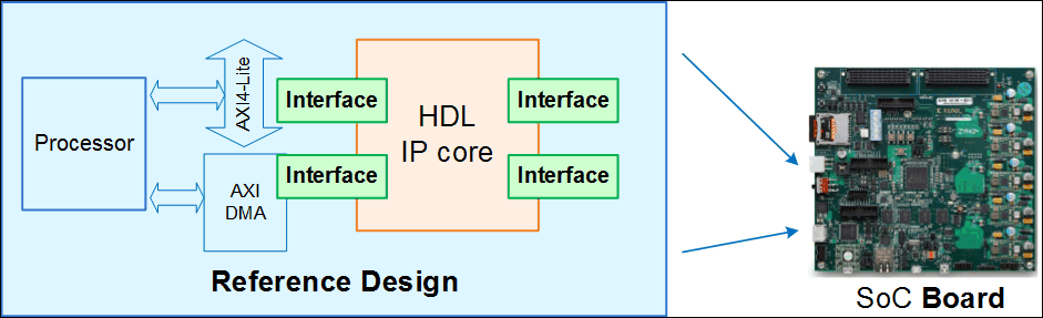
A reference design captures the complete structure of an SoC design, defining the different components and their interconnections. The HDL Coder SoC workflow generates an IP core that integrates with the reference design, and is then used to program an SoC board. This figure shows the relationship between a reference design, an HDL IP core, and an SoC board.
To create and export a simple reference design by using the Xilinx Vivado IP Integrator environment, follow these steps. For more information about the IP Integrator tool, refer to Xilinx documentation.
1. Create an empty Xilinx Vivado RTL project by using board part Z********************************ybo Z7-10 or Zybo Z7-20 as the default board.

2. Create an empty block design and add the Z********************************YNQ7 Processing System IP block. Run block automation to set a board preset for Zybo Z7-10 or Zybo Z7-20, which contains the parameters for ZYNQ7 Processing system IP related to MIO Configuration, Clock configuration, and DDR Configuration.

The MIO peripherals have been marked in accordance with the Zybo board definition as the result of applying a board preset.

3. Complete the block design.
Notice that the block design does not contain any information about the HDL IP core.
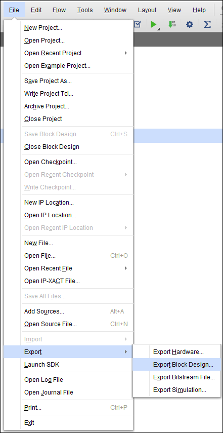
4. Export the completed block design as a Tcl script design_led.tcl by selecting File > Export > Export Block Design.
The exported Tcl script (design_led.tcl) constitutes the custom reference design. The Tcl script is used in the HDL Coder SoC workflow to recreate the block design and integrate the generated HDL IP core with the block design in a Xilinx Vivado project. This completes the process of creation and export of custom reference design using Xilinx Vivado.
Register the Zybo Z7-10 or Zybo Z7-20 Board in HDL Workflow Advisor
The process involves the creation of board registration file and board definition files.
1. Create a board registration file.
Create a board registration file with the name hdlcoder_board_customization.m and add it to the MATLAB path.
A board registration file contains a list of board plugins. A board plugin is a MATLAB package folder containing a board definition file and all reference design plugins associated with the board.
This code describes the contents of a board registration file that contains the board plugin ZyboZ710Registration and ZyboZ720Registration to register the Zybo board in HDL Workflow Advisor.
function r = hdlcoder_board_customization
% Board plugin registration file
% 1. Any registration file with this name on MATLAB path will be picked up
% 2. Registration file returns a cell array pointing to the location of
%    the board plugins
% 3. Board plugin must be a package folder accessible from MATLAB path,
%    and contains a board definition file
r = { ...
      'ZyboZ710Registration.plugin_board', ...
      'ZyboZ720Registration.plugin_board'
     };
end
2. Create the board definition file.
A board definition file contains information about the SoC board.
Zybo Z7-10
This code describes the contents of the Zybo board definition file plugin_board.m that resides inside the board plugin folder ZyboZ710Registration.
Information about the FPGA I/O pin locations ('FPGAPin') and standards ('IOSTANDARD') is obtained from the Zybo master constraints file from the Digilent website.
The property BoardName defines the name of the Zybo Z7-10 board as ZYBO Z7-10 in HDL Workflow Advisor.
function hB = plugin_board()
% Board definition
% Construct board object
hB = hdlcoder.Board;
hB.BoardName = 'ZYBO Z7-10';
% FPGA device information
hB.FPGAVendor   = 'Xilinx';
hB.FPGAFamily   = 'Zynq';
hB.FPGADevice   = 'xc7z010';
hB.FPGAPackage  = 'clg400';
hB.FPGASpeed    = '-1';
% Tool information
hB.SupportedTool = {'Xilinx Vivado'};
% FPGA JTAG chain position
hB.JTAGChainPosition = 2;
%% Add interfaces
% Standard "External Port" interface
hB.addExternalPortInterface( ...
    'IOPadConstraint', {'IOSTANDARD = LVCMOS33'});
% Custom board external I/O interface
hB.addExternalIOInterface( ...
  'InterfaceID',    'LEDs General Purpose', ...
  'InterfaceType',  'OUT', ...
  'PortName',       'LEDs', ...
  'PortWidth',      4, ...
  'FPGAPin',        {'M14', 'M15', 'G14', 'D18'}, ...
  'IOPadConstraint', {'IOSTANDARD = LVCMOS33'});
hB.addExternalIOInterface( ...
   'InterfaceID',    'Push Buttons', ...
   'InterfaceType',  'IN', ...
   'PortName',       'PushButtons', ...
   'PortWidth',      4, ...
   'FPGAPin',        {'K18', 'P16', 'K19', 'Y16'}, ...
   'IOPadConstraint', {'IOSTANDARD = LVCMOS33'});
hB.addExternalIOInterface( ...
   'InterfaceID',    'Slide switches ', ...
   'InterfaceType',  'IN', ...
   'PortName',       'SlideSwitches', ...
   'PortWidth',      4, ...
   'FPGAPin',        {'G15', 'P15', 'W13', 'T16'}, ...
   'IOPadConstraint', {'IOSTANDARD = LVCMOS33'});
Zybo Z7-20
This code describes the contents of the Zybo board definition file plugin_board.m that resides inside the board plugin folder ZyboZ720Registration.
The property BoardName defines the name of the Zybo Z7-20 board as ZYBO Z7-20 in HDL Workflow Advisor.
function hB = plugin_board()
% Board definition

%   Copyright 2024 The MathWorks, Inc.

% Construct board object
hB = hdlcoder.Board;

hB.BoardName    = 'ZYBO Z7-20';

% FPGA device information
hB.FPGAVendor   = 'Xilinx';
hB.FPGAFamily   = 'Zynq';
hB.FPGADevice   = 'xc7z020';
hB.FPGAPackage  = 'clg400';
hB.FPGASpeed    = '-1';

% Tool information
hB.SupportedTool = {'Xilinx Vivado'};

% FPGA JTAG chain position
hB.JTAGChainPosition = 2;

%% Add interfaces
% Standard "External Port" interface
hB.addExternalPortInterface( ...
    'IOPadConstraint', {'IOSTANDARD = LVCMOS33'});

% Custom board external I/O interface
hB.addExternalIOInterface( ...
    'InterfaceID',    'LEDs General Purpose', ...
    'InterfaceType',  'OUT', ...
    'PortName',       'LEDs', ...
    'PortWidth',      4, ...
    'FPGAPin',        {'M14', 'M15', 'G14', 'D18'}, ...
    'IOPadConstraint', {'IOSTANDARD = LVCMOS33'});

hB.addExternalIOInterface( ...
     'InterfaceID',    'Push Buttons', ...
     'InterfaceType',  'IN', ...
     'PortName',       'PushButtons', ...
     'PortWidth',      4, ...
     'FPGAPin',        {'K18', 'P16', 'K19', 'Y16'}, ...
     'IOPadConstraint', {'IOSTANDARD = LVCMOS33'});

 hB.addExternalIOInterface( ...
	'InterfaceID',    'Slide switches ', ...
	'InterfaceType',  'IN', ...
	'PortName',       'SlideSwitches', ...
	'PortWidth',      4, ...
	'FPGAPin',        {'G15', 'P15', 'W13', 'T16'}, ...
	'IOPadConstraint', {'IOSTANDARD = LVCMOS33'});

% LocalWords:  ZYBO Zynq xc Vivado JTAG IOSTANDARD LVCMOS
This completes the process of registering custom board plugins with the HDL Workflow Advisor. Now you can continue registering the custom reference design that have been created earlier in the HDL Workflow Advisor in next section.
Register the Custom Reference Design in HDL Workflow Advisor
This section explains how you can register the custom reference designs with the HDL Workflow Advisor. The process involves the creation of custom reference design registration file and custom reference design definition file.
1. Create reference design registration file.
Create a reference design registration file named hdlcoder_ref_design_customization.m containing a list of reference design plugins associated with an SoC board.
A reference design plugin is a MATLAB package folder containing the reference design definition file and all files associated with the SoC design project. A reference design registration file must also contain the name of the associated board.
Zybo Z7-10
This code describes the contents of a Zybo reference design registration file containing the reference design plugin ZyboZ710Registration.Vivado2020_2 and ZyboZ710Registration.Vivado2022_1 associated with the board ZYBO Z7-10 depending on the Vivado tool version you are registering with the MATLAB path. Note that the folder name may not directly indicate the Vivado version that is being supported. Currently, there are two custom reference designs supporting as shown below.
function [rd, boardName] = hdlcoder_ref_design_customization
% Reference design plugin registration file
% 1. The registration file with this name inside of a board plugin folder
%    will be picked up
% 2. Any registration file with this name on MATLAB path will also be picked up
% 3. The registration file returns a cell array pointing to the location of
%    the reference design plugins
% 4. The registration file also returns its associated board name
% 5. Reference design plugin must be a package folder accessible from
%    MATLAB path, and contains a reference design definition file
rd = {
      'ZyboZ710Registration.Vivado2020_2.plugin_rd', ...
      'ZyboZ710Registration.Vivado2022_1.plugin_rd', ...
      'ZyboZ710Registration.Vivado_Audio_filter_2020_2.plugin_rd', ...
      'ZyboZ710Registration.Vivado_Audio_filter_2022_1.plugin_rd'

     };
boardName = 'ZYBO Z7-10';
end
Zybo Z7-20
This code describes the contents of a Zybo reference design registration file containing the reference design plugin ZyboZ720Registration.Vivado2023_1 associated with the board ZYBO Z7-20 depending on the Vivado tool version you are registering with the MATLAB path. The support for ZYBO Z7-20 board has been added newly using Xilinx Vivado tool version 2023.1, hence the folder name contains Vivado2023_1.
function [rd, boardName] = hdlcoder_ref_design_customization
% Reference design plugin registration file
% 1. The registration file with this name inside of a board plugin folder
%    will be picked up
% 2. Any registration file with this name on MATLAB path will also be picked up
% 3. The registration file returns a cell array pointing to the location of
%    the reference design plugins
% 4. The registration file also returns its associated board name
% 5. Reference design plugin must be a package folder accessible from
%    MATLAB path, and contains a reference design definition file

%   Copyright 2024 The MathWorks, Inc.

rd = { 'ZyboZ720Registration.Vivado2023_1.plugin_rd', ...

     };

boardName = 'ZYBO Z7-20';
end

% LocalWords:  plugins Zybo Vivado ZYBO
2. Create the reference design definition file.
A reference design definition file defines the interfaces between the custom reference design and the HDL IP core that is generated by the HDL Coder SoC workflow.
Zybo Z7-10
This code describes the contents of the Zybo Z7-10 reference design definition file plugin_rd.m associated with the board ZYBO Z7-10 that resides inside the reference design plugin ZyboZ710Registration.Vivado2022_1. The property ReferenceDesignName defines the name of the reference design as Demo system in HDL Workflow Advisor.
function hRD = plugin_rd()
% Reference design definition
% Construct reference design object
hRD = hdlcoder.ReferenceDesign('SynthesisTool', 'Xilinx Vivado');
hRD.ReferenceDesignName = 'Demo system';
hRD.BoardName = 'ZYBO Z7-10';
% Tool information
hRD.SupportedToolVersion = {'2022.1','2023.1'};
% add custom Vivado design
hRD.addCustomVivadoDesign( ...
    'CustomBlockDesignTcl', 'design_led.tcl', ...
    'VivadoBoardPart','digilentinc.com:zybo-z7-10:part0:1.0');
%% Add interfaces
% add clock interface
hRD.addClockInterface( ...
  'ClockConnection',   'core_clkwiz/clk_out1', ...
  'ResetConnection',   'sys_core_rstgen/peripheral_aresetn');
% add Register interfaces
hRD.addRegisterInterface( ...
    'InterfaceConnection', 'axi_cpu_interconnect/M00_AXI', ...
    'BaseAddress',         '0x40010000', ...
    'MasterAddressSpace',  'sys_cpu/Data');
hRD.DeviceTreeName = 'devicetree_axilite.dtb';
A reference design plugin must also contain the SoC design project files.
The Zybo reference design plugin folder ZyboZ710Registration.Vivado2022_1 must contain the Tcl script design_led.tcl exported previously from the Xilinx Vivado project. The Zybo reference design definition file plugin_rd.m identifies the SoC design project file through this statement:
hRD.addCustomVivadoDesign('CustomBlockDesignTcl', 'design_led.tcl');
plugin_rd.m also defines the interface connections between the custom reference design and the HDL IP core indicated by these statements:
hRD.addClockInterface( ...
  'ClockConnection',   'core_clkwiz/clk_out1', ...
  'ResetConnection',   'sys_core_rstgen/peripheral_aresetn');
hRD.addRegisterInterface( ...
    'InterfaceConnection', 'axi_cpu_interconnect/M00_AXI', ...
    'BaseAddress',         '0x40010000', ...
    'MasterAddressSpace',  'sys_cpu/Data');
Note The 'BaseAddress' of the AXI4 interface must be a valid address in the 'MasterAddressSpace'. The address must not create any address conflict with other address-based peripherals in the custom reference design.
Zybo Z7-20
This code describes the contents of the Zybo Z7-20 reference design definition file plugin_rd.m associated with the board ZYBO Z7-20 that resides inside the reference design plugin ZyboZ720Registration.Vivado2023_1. The property ReferenceDesignName defines the name of the reference design as Demo system in HDL Workflow Advisor.
function hRD = plugin_rd()
% Reference design definition

%   Copyright 2024 The MathWorks, Inc.

% Construct reference design object
hRD = hdlcoder.ReferenceDesign('SynthesisTool', 'Xilinx Vivado');

hRD.ReferenceDesignName = 'Demo system';
hRD.BoardName = 'ZYBO Z7-20';

% Tool information
hRD.SupportedToolVersion = {'2023.1'};

% add custom Vivado design
hRD.addCustomVivadoDesign( ...
    'CustomBlockDesignTcl', 'design_led.tcl', ...
    'VivadoBoardPart',      'digilentinc.com:zybo-z7-20:part0:1.1');

%% Add interfaces
% add clock interface
hRD.addClockInterface( ...
    'ClockConnection',   'core_clkwiz/clk_out1', ...
    'ResetConnection',   'sys_core_rstgen/peripheral_aresetn');

% add Register interfaces
hRD.addRegisterInterface( ...
    'InterfaceConnection', 'axi_cpu_interconnect/M00_AXI', ...
    'BaseAddress',         '0x40010000', ...
    'MasterAddressSpace',  'sys_cpu/Data');

hRD.DeviceTreeName = 'devicetree_axilite.dtb';

% LocalWords:  Vivado ZYBO Tcl tcl digilentinc zybo wiz proc aresetn AXI axi
% LocalWords:  devicetree axilite dtb
Execute the SoC Workflow for the Zybo Board
Use the custom board and reference design registration system to generate an HDL IP core that blinks LEDs on the Zybo Z7-10/Zybo Z7-20 board. The required files used are located in the ZYBO folder.
1. Add the Zybo board registration file to the MATLAB path.
example_root = (hdlcoder_amd_examples_root)
cd (example_root)
addpath(genpath('ZYBO'));
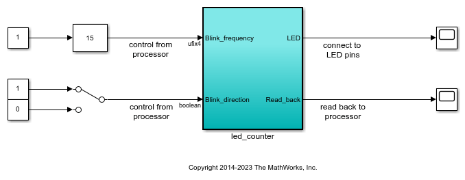
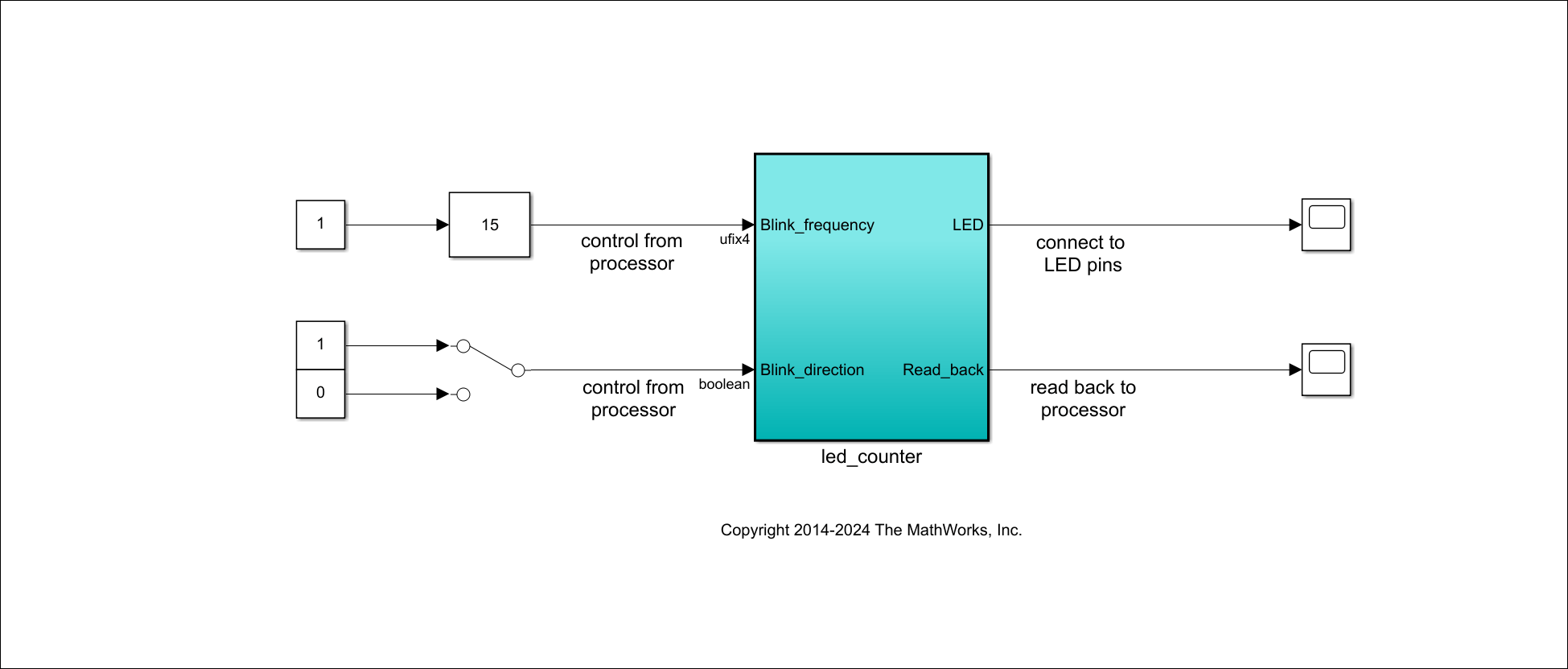
2. Open the Simulink model that implements LED blinking.
open_system('hdlcoder_led_blinking_4bit');
3. Select the hdlcoder_led_blinking_4bit/led_counter subsystem. On the Apps tab, click HDL Coder. On the HDL Code tab, in the Assistance section, click Workflow Advisor to open the HDL Workflow Advisor.
4. In the Set Target > Set Target Device and Synthesis Tool task, select IP Core Generation for the Target workflow. ZYBO Z7-10 now appears in the drop-down list Target Platform. Select ZYBO Z7-10 as a Target Platform. You can also choose the Target Platform as ZYBO Z7-20 as the support has been provided to this board newly in HDL Coder Support Package for AMD FPGA and SoC Devices.
5. Click Run This Task to complete the Set Target Device and Synthesis Tool task.
6. In the Set Target > Set Target Reference Design task, the custom reference design Demo system now appears in the Reference design field. Select Demo system and click Run This Task.
7. In Task 1.3 Set Target Interface, select the connections, and then click on Run This Task.
8. To generate IP core and view the IP core generation report, follow step 3 and step 4 of Generate an HDL IP core using the HDL Workflow Advisor section of Get Started with IP Core Generation from Simulink Model.
9. To integrate the IP core in the reference design and create the vivado project, follow step 1 of Integrate the IP core with the Xilinx Vivado environment section of Get Started with IP Core Generation from Simulink Model.
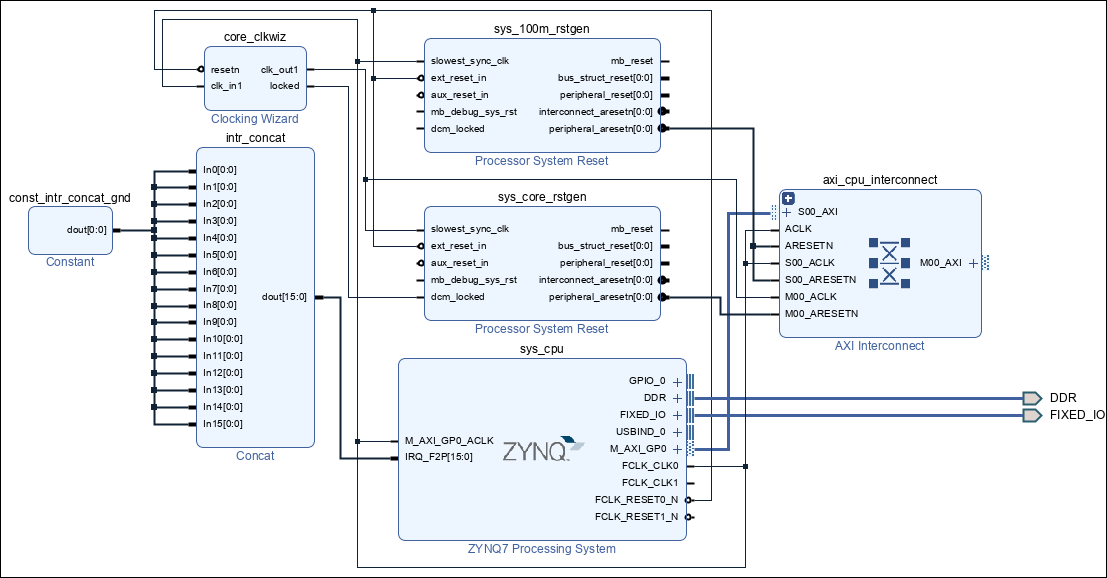
10. After completing the Create Project task under Embedded System Integration, examine the Xilinx Vivado project created by the SoC workflow. This figure shows the block design of the SoC project where you have highlighted the HDL IP Core. Compare this block design with the previous block design used to export the custom reference design for a deeper understanding of the relationship between a custom reference design and an HDL IP Core.
11. Follow the steps 2, 3 and 4 of Integrate the IP core with the Xilinx Vivado environment section of Get Started with IP Core Generation from Simulink Model example to generate the software interface model, generate the FPGA bitstream, and program the target device respectively.
12. After loading the bitstream, the LEDs on the Zybo Z7-10 or Zybo Z7-20 board now start blinking. You can control the LED blink frequency and direction by executing the software interface model on the Zynq ARM processor. Refer to Generate a software interface model section of Get Started with IP Core Generation from Simulink Model example to control the LED blink frequency and direction from the generated software interface model.
Summary
This example shows how to define and register a custom board for Zynq workflow in HDL Workflow Advisor. This example also explains the process of creation and exporting a custom reference design using Xilinx Vivado and register the reference design in HDL Workflow Advisor.