Create RFSoC HDL Coder Models
This workflow customizes and designs an RFSoC model using the Zynq RFSoC Template Builder tool.
This figure shows all of the interfaces that you can model by using the Xilinx® Zynq® UltraScale+™ RFSoC ZCU111 and Xilinx Zynq UltraScale+ RFSoC ZCU216 evaluation kits.
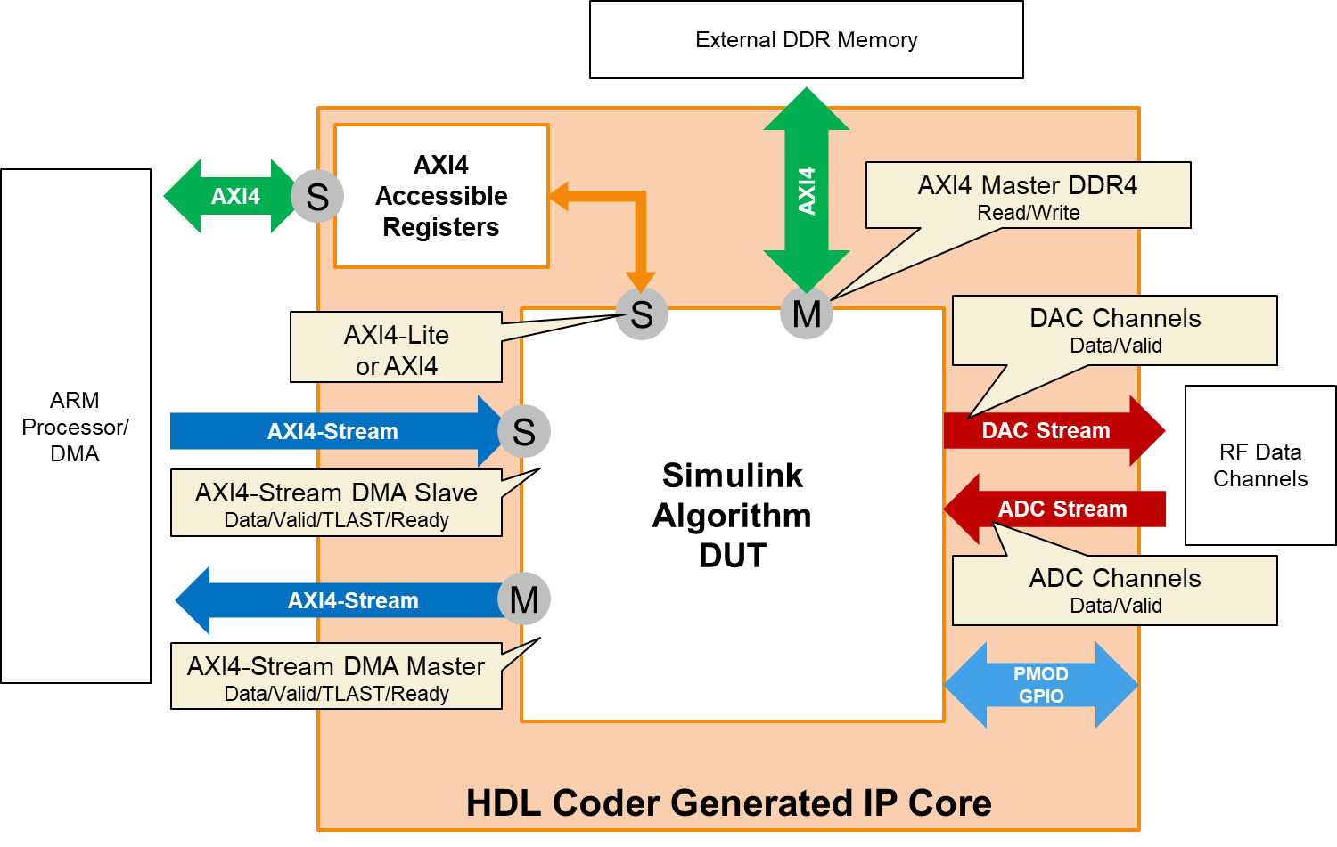
In this workflow, because the generated IP core interfaces with both analog-to-digital converter (ADC) and digital-to-analog converter (DAC) RFSoC tiles, the FPGA clock rate uses a compatible clock domain. Differing ADC and DAC sampling rates are possible, but you can choose the interpolation and decimation rates and samples per clock to result in a common FPGA clock rate.
| Reference Design Parameter | Value |
|---|---|
| ADC sampling rate (MHz) | 4096 |
| ADC decimation mode (xN) | 8 |
| ADC samples per clock cycle | 2 |
| DAC sampling rate (MHz) | 1024 |
| DAC interpolation mode (xN) | 4 |
| DAC samples per clock cycle | 1 |
The ADC and DAC clock rates are calculated as:
ADC clock rate = 4096/8/2 = 256 MHz
DAC clock rate = 1024/4/1 = 256 MHz
In this example, the HDL Coder™ IP core runs at 256 MHz. If the clock domains do not match, an error emits in the HDL Coder reference design workflow.
Because different types of designs exist that can map to different tiles and channels, building a model from a new model can be time-consuming. To generate a model based on the selected reference design, use the Zynq RFSoC Template Builder tool. To open this tool, enter one of these commands at the MATLAB® command prompt.
rfsocTemplateBuilder('zcu111')— Generate an RFSoC model for a ZCU111 board.rfsocTemplateBuilder('zcu216')— Generate an RFSoC model for a ZCU216 board.
This figure shows the Zynq RFSoC Template Builder tool window.
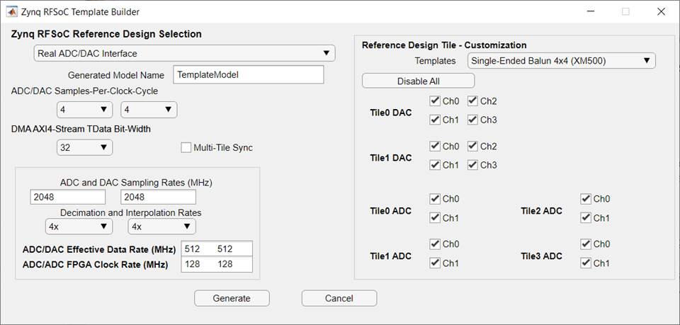
Select Reference Design
In the Zynq RFSoC Reference Design Selection pane, select a reference design that maps to different parts of the RFSoC tiles.
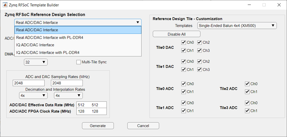
Real ADC/DAC Interface— Select this option when your design receives and transmits real data.Real ADC/DAC Interface with PL-DDR4— Select this option when your design receives and transmits real data, and uses DDR4 buffering. Selecting this option adds an AXI4 interface to your device under test (DUT) for connection to the DDR4 memory.IQ ADC/DAC Interface— Select this option when your design receives and transmits complex in-phase and quadrature (IQ) data.IQ ADC/DAC Interface with PL-DDR4— Select this option when your design receives and transmits complex IQ data and uses DDR4 buffering. Selecting this option adds an AXI4 interface to your DUT for connection to the DDR4 memory.
Customize Reference Design Tiles
In the Reference Design Tile - Customization pane, you can customize the channel mapping of your model. The Templates parameter provides the preconfigured channel mappings. The template options depend on the board type. This figure shows the available templates for a ZCU111 board.
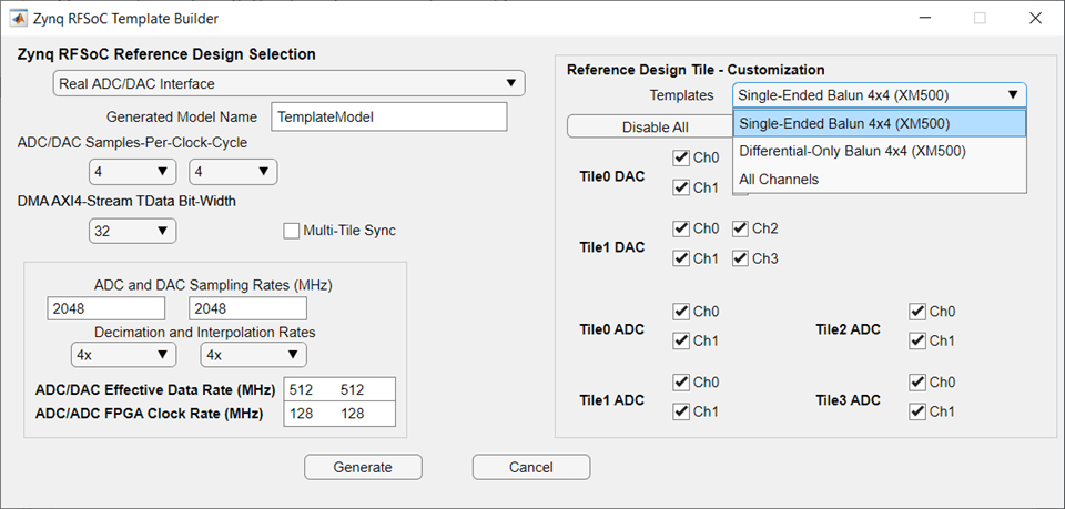
These templates reflect the XM500 balun board and the different differential versus single-ended connectors.
Single-Ended Balun 4x4 (XM500)— This option includes Tile1 DAC, Tile0 ADC, and Tile1 ADC. These connectors require only a single subminiature version A (SMA) connector per channel, however, they also connect to several RF cages that act as lowpass or highpass filters. When you build your design, you must take these into consideration.Differential-Only 4x4 (XM500)— This option includes Tile0 DAC, Tile2 ADC, and Tile3 ADC. These connectors require differential SMA connections with the adaptors such as DC blockers. Because an RF filter is not applied on the channel (unlike the single-ended SMA), using this option can be useful for testing designs that have a wide frequency range or when phase alignment is important.All Channels— This option selects all eight DAC and eight ADC channels for mapping.
Configure Sample Rates and Data Width
In the Zynq RFSoC Reference Design Selection pane, you can further customize various RFSoC parameters, such as sampling rates or decimation and interpolation factors.
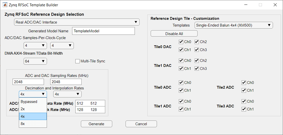
Set the ADC/DAC Samples-Per-Clock-Cycle parameter to the required
sample rate. Set the DMA AXI4-Stream TData Bit-Width parameter to
32, 64, or
128 bits. The number of samples per clock, or DMA data width,
affect the data type of the signal lines to reflect the word
length. For example, when you specify 4 samples per clock, the word length for the ADC or
DAC input and output (I/O) lines is 64 bits because each sample is 16 bits. To enable
multi-tile synchronization (MTS), select the Multi-Tile Sync parameter.
Enabling MTS has specific requirements. For more information on MTS mode, see Zynq UltraScale+ RFSoC RF Data Converter v2.3 in the Xilinx documentation.
Click Generate. A generated template model opens in a Simulink® window. The template model maps the input and output ports to the various ADC and DAC tiles that are associated with the RFSoC device. Double-click the model and add logic to reflect your algorithm.
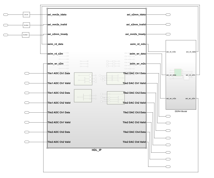
After you create an RFSoC model using the Zynq RFSoC Template Builder tool, use the HDL Workflow Advisor and follow the IP core generation workflow to generate an HDL IP, build a bitstream, and program a ZCU111 or ZCU216 board.
The HDL Workflow Advisor shows the design parameters that you specified in the Zynq RFSoC Template Builder tool. You can adjust the parameters as needed for the channel mapping. The preceding generated model is copied to the MATLAB current working folder. The inport and outport blocks are stubbed out, leaving space for your DSP design.