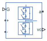
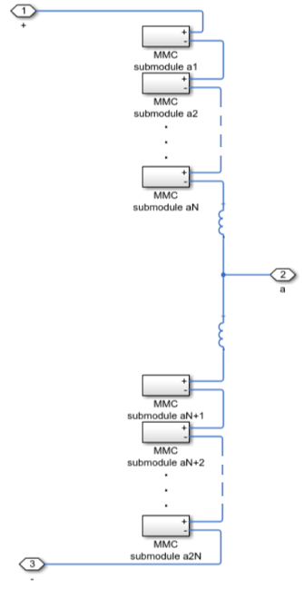
Modular Multilevel Converter Leg
Modular multilevel converter leg with series-connected power submodules
Libraries:
Simscape /
Electrical /
Semiconductors & Converters /
Converters
Description
The Modular Multilevel Converter Leg block models a modular multilevel converter leg as a two arms that are implemented with a number of series-connected power submodules.
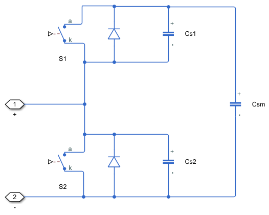
Half-Bridge Topology
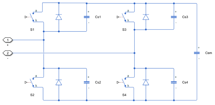
Full-Bridge Topology
This blocks allows you to select the level of model fidelity by choosing between a detailed model with switching devices or an equivalent model. You can choose from these switching devices are:
GTO — Gate turn-off thyristor. For information about the I-V characteristic of the device, see GTO.
Ideal semiconductor switch — For information about the I-V characteristic of the device, see Ideal Semiconductor Switch.
IGBT — Insulated-gate bipolar transistor. For information about the I-V characteristic of the device, see IGBT (Ideal, Switching).
MOSFET — N-channel metal-oxide-semiconductor field-effect transistor. For information about the I-V characteristic of the device, see MOSFET (Ideal, Switching).
Thyristor — For information about the I-V characteristic of the device, see Thyristor (Piecewise Linear).
Averaged Switch — Semiconductor switch with an antiparallel diode. The control signal port G accepts values in the interval [0,1]. When G is equal to
0or1, the averaged switch is fully opened or fully closed respectively. The switch behaves similarly to the Ideal Semiconductor Switch block with an antiparallel diode. When G is between 0 and 1, the averaged switch is partly opened. You can average the pulse-width modulation (PWM) signal over a specified period. You can then undersample the model or use modulation waveforms instead of PWM signals.
Piecewise Constant Approximation in Averaged Switch for FPGA Deployment
If you set the Switching device parameter to Averaged switch and your model uses a partitioning solver, this block produces nonlinear partitions because the average mode equations include modes, Gsat that are functions of the input G. To make these equations compatible with hardware description language (HDL) code generation, and therefore FPGA deployment, set the Integer for piecewise constant approximation of gate input (0 for disabled) parameter to a value greater than 0. This block then treats the Gsat mode as a piecewise constant integer with a fixed range. This turns the previously nonlinear partitions to linear time varying partitions.
An integer value in the range [0,K], where K is the value of the Integer for piecewise constant approximation of gate input (0 for disabled), is now associated with each real value mode in the range [0,1]. The block computes the piecewise constant mode by dividing the original mode by K to normalize it back to the range [0,1]:
Variables
To set the priority and initial target values for the block variables before simulation, use the Initial Targets section in the block dialog box or Property Inspector. For more information, see Set Priority and Initial Target for Block Variables.
Nominal values provide a way to specify the expected magnitude of a variable in a model. Using system scaling based on nominal values increases the simulation robustness. You can specify nominal values using different sources, including the Nominal Values section in the block dialog box or Property Inspector. For more information, see System Scaling by Nominal Values.
Ports
Input
Output
Conserving
Parameters
References
[1] Saad, Hani, Sebastien Dennetiere, and Jean Mahseredjian. “On Modelling of MMC in EMT-Type Program.” 2016 IEEE 17th Workshop on Control and Modeling for Power Electronics (COMPEL), 1–7. Trondheim, Norway: IEEE, 2016. https://doi.org/10.1109/COMPEL.2016.7556717.
Extended Capabilities
Version History
Introduced in R2020b
See Also
Average-Value DC-DC Converter | Bidirectional DC-DC Converter | Buck Converter | Buck-Boost Converter | Converter (Three-Phase) | GTO | IGBT (Ideal, Switching) | MOSFET (Ideal, Switching) | Ideal Semiconductor Switch | PWM Generator | PWM Generator (Three-phase, Two-level) | Three-Level Converter (Three-Phase) | Thyristor (Piecewise Linear) | Boost Converter | Modular Multilevel Converter Arm | Modular Multilevel Converter (Three-Phase) | PWM Generator (Multilevel)