Get Started with IP Core Generation for Intel Quartus Pro Based Devices
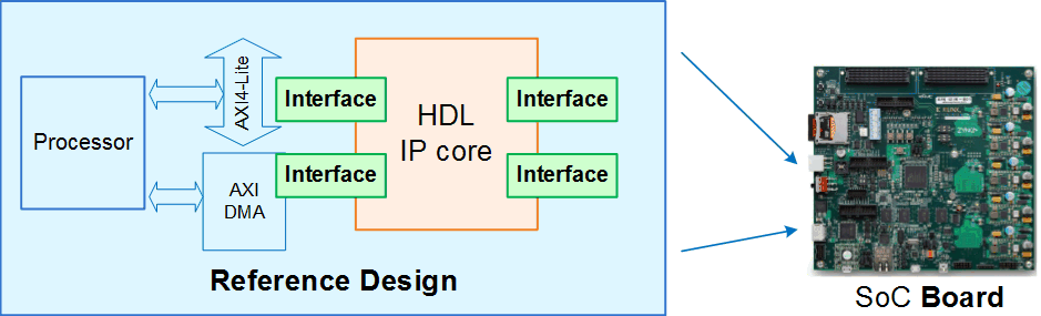
This example shows how to build a reference design by using Intel® Platform Designer® and then deploy the design to an Intel® Arria 10 SoC. A reference design defines the SoC architecture, including components and their connections. When you create a reference design, HDL Coder generates an IP core that uses the reference design to program the SoC board.
In this example, you create a reference design that blinks LEDs at different frequencies. You create a reference design, export design to a Tcl script, set up the SoC board, generate the HDL IP core, and deploy it to the SoC board. This figure illustrates how the reference design, HDL IP core, and SoC board work together.
Prerequisites
Install and set up the following tools and hardware:
Intel® Quartus® Pro synthesis tool. For a list of supported versions, see HDL Language Support and Supported Third-Party Tools and Hardware.
Intel Arria 10 SoC development kit.
HDL Coder Support Package for Intel FPGA and SoC Devices.
Embedded Coder Support Package for Intel SoC Devices.
Build Reference Design in Intel Platform Designer
First, create and export the reference design.
Launch Intel Quartus Pro and create a project that targets Intel Arria 10 SoC development kit.
Open Platform Designer and build the reference design by including these IP cores:
Clock Bridge Intel FPGA IP
Reset Bridge Intel FPGA IP
IOPLL Intel FPGA IP
Hard Processor System Intel Arria10 FPGA IP
Optionally, set the design clock to 50 MHz or configure the IOPLL output clock to meet your application requirements. The IOPLL output clock drives the IP core of the DUT. You can also specify the target clock frequency in the
plugin_rd.mfile.
In Platform Designer, you can set the Instance name and HDL entity name parameter for each IP core. By default, the HDL entity name is system_soc, followed by the instance name. For example, if the instance name is iopll_0, then the corresponding HDL entity name is system_soc_iopll_0.
If you want the HDL entity name to match the instance name exactly, you can manually set the HDL entity name when you add the IP to the reference design. After you add the IP, the HDL entity name becomes fixed and cannot be changed. However, you can modify the instance name at any time.
Export Reference Design to Tcl Script
Next, export the reference design to a Tcl script.
Open the completed design in Platform Designer.
Select File > Export System as Platform Designer Script.
Save the Tcl script to your project directory.
The Tcl script records the reference design structure and configuration, including IP instances such as the clock source, Intel IOPLL, and external memory interface. At this stage, the HDL Coder generated DUT IP is not part of the reference design.
Register Reference Design in Board Plugin file
Register the exported Tcl script in the board plugin.
Open the
plugin_rd.mfile in the(matlabroot)/toolbox/hdlcoder/boards/intel/+IntelArria10SoC/+qpro_base_24_2folder.Use the
hRD.addCustomQsysDesignAPI to register the reference design.Verify that the path and naming conventions match your board and reference design configuration.
Define DUT Connections in the Board Plugin file
In the plugin_rd.m file, you explicitly define all connections to the DUT IP by using HDL Coder reference design registration APIs. Make these changes to match your design file:
Use the
hRD.addClockInterfaceAPI to specify the clock connection for the DUT. To connect the DUT IP clock to theoutclk0output, set theClockConnectionparameter tooutclk0.Define the clock frequency and supported ranges in the same API call. These values represent the operating frequencies supported by the DUT IP. You can modify the default frequency to your desired target frequency directly in the
plugin_rd.mfile.
In the plugin_rd.m file, the ClockModuleInstance has the name arria10_iopll. This name refers to the HDL entity name of the IOPLL IP, not its instance.
You can use this reference design to create an HDL IP Core to blink the LEDs on the Intel Arria10 SoC development kit. For more information, see Get Started with IP Core Generation for Intel SoC Devices.
Enable Early I/O Release
To reduce boot time by allowing DDR and shared I/O access before programming the FPGA fabric, enable early I/O release. In the plugin_rd.m file, set the hRD.GenerateSplitBitstream parameter to true.
This setting splits the FPGA configuration into two stages:
Peripheral configuration: Configures the FPGA I/O, shared I/O, and enables the HPS External Memory Interface (EMIF).
Core configuration: Configures the FPGA fabric.
By splitting the FPGA configuration, the Intel Arria10 SoC HPS can access the shared I/O and EMIF earlier, which enables faster boot or alternate boot sources.
When you enable this feature, HDL Coder generates two RBF files:
The
peripheral.rbffile configures FPGA I/O, shared I/O, and HPS EMIF.The
core.rbffile completes FPGA fabric configuration.
Load the peripheral.rbf file first, then the core.rbf file. The peripheral.rbf file releases the HPS EMIF pins and begins calibration.
Prepare Hardware and Install Tools
Next, set up the hardware and install the required tools.
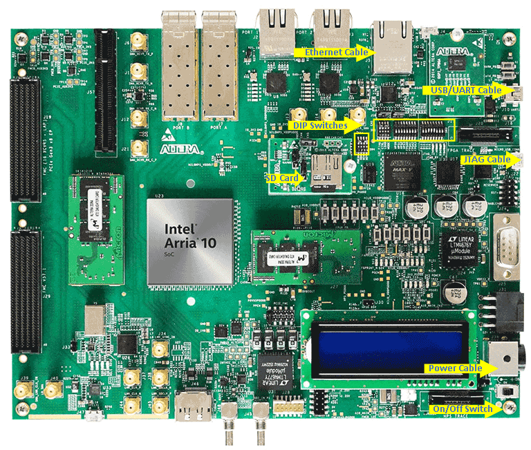
1. Set up the Arria 10 SoC as shown in the figure below. To learn more about the Arria 10 SoC hardware setup, refer to the board documentation.
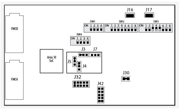
2. Configure the DIP switches and jumper settings as shown in the figure below.
3. Connect the USB-UART port to your computer by using a Micro-USB cable. Install the FTDI USB-to-UART drivers, if needed.
4. Connect the board to your computer by using an Ethernet cable.
5. Install the required support packages.
In MATLAB, in the Home tab, click Add-Ons > Get Hardware Support Packages.
Install these support packages:
HDL Coder Support Package for Intel FPGA and SoC Devices
Embedded Coder Support Package for Intel SoC Devices
6. Ensure that you are using the SD card image provided by the Embedded Coder Support Package for Intel SoC Devices. If you need to update your SD card image, see the Hardware Setup section of Add Support for Intel SoC Platform (Embedded Coder).
7. Create a hardware connection by entering:
h = alterasoc("IPAddress","Username","Password");
The alterasoc function logs in to the hardware via the COM port and runs the ifconfig command to obtain the IP address of the board. This function also tests the Ethernet connection.
8. Optionally, test the serial connection by using this configuration and a program such as PuTTY™.
Baud rate:
115200Data bits:
8Stop bits:
1Parity:
NoneFlow control:
None
If this connection is successful, the serial console displays Linux boot log when you power cycle the Intel® Arria® 10 SoC board. Close the serial connection before using the alterasoc function again.
9. Set the path to your Intel Quartus Pro synthesis tool by using the hdlsetuptoolpath function. Specify your Quartus installation path when you run the command.
hdlsetuptoolpath("ToolName", "Intel Quartus Pro", "ToolPath", "C:\Altera\24.2_pro\Windows\quartus\bin64");
Open Model
Open the hdlcoder_led_blinking_4bit model.
modelname = "hdlcoder_led_blinking_4bit";
open_system(modelname);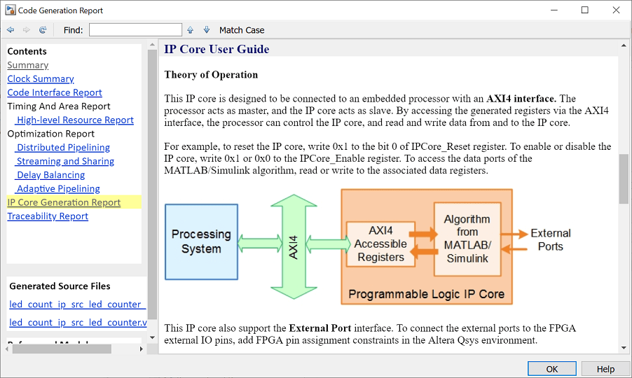
Partition your Simulink® model into hardware and software components.
Decide which parts of the design to implement on programmable logic and which parts to run on the ARM® processor.
Group all the blocks for programmable logic into an atomic subsystem. This atomic subsystem defines the hardware-software boundary:
Blocks inside the subsystem run on programmable logic.
Blocks outside this subsystem run on the ARM processor.
In this example:
The
led_countersubsystem is the hardware subsystem. It implements a counter that blinks LEDs on the FPGA board.Control ports
Blink_frequencyandBlink_directiondetermine the LED blink frequency and direction.The Slider Gain or Manual Switch blocks adjust the input values.
The output port of the
led_countersubsystem, LED connects to the LED hardware, and the output port Read_Back returns data to the processor.The blocks outside of the
led_countersubsystem run in software. The ARM processor controls the generated IP core by writing to the AXI-accessible registers.
Generate an HDL IP core by Using the HDL Workflow Advisor
Next, use the HDL Workflow Advisor to create a reusable IP core module from your Simulink model. HDL Coder generates HDL code for the model and AXI interface logic, then packages the files into an IP core folder for integration with Intel Platform Designer.
Set Target Device and Synthesis Tool
Launch HDL Workflow Advisor. In the Apps tab, click HDL Coder. In the HDL Code tab, click Workflow Advisor.
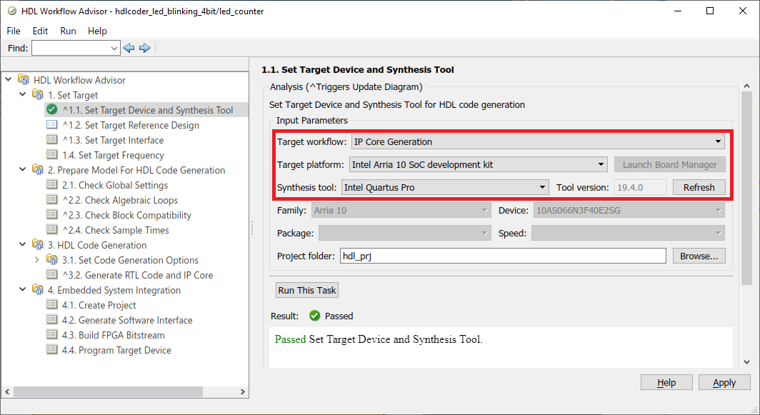
In task 1.1 Set Target Device and Synthesis Tool:
Set Target workflow to
IP Core Generation.Set Target platform to
Intel Arria 10 SoC development kit. If you do not see this option, clickGet moreto open the Support Package Installer. In the Support Package Installer, select Intel FPGA and SoC Devices and follow the instructions to complete the installation.Set Synthesis tool to
Intel Quartus Pro.Click Run This Task.
Configure Target Interface and Frequency
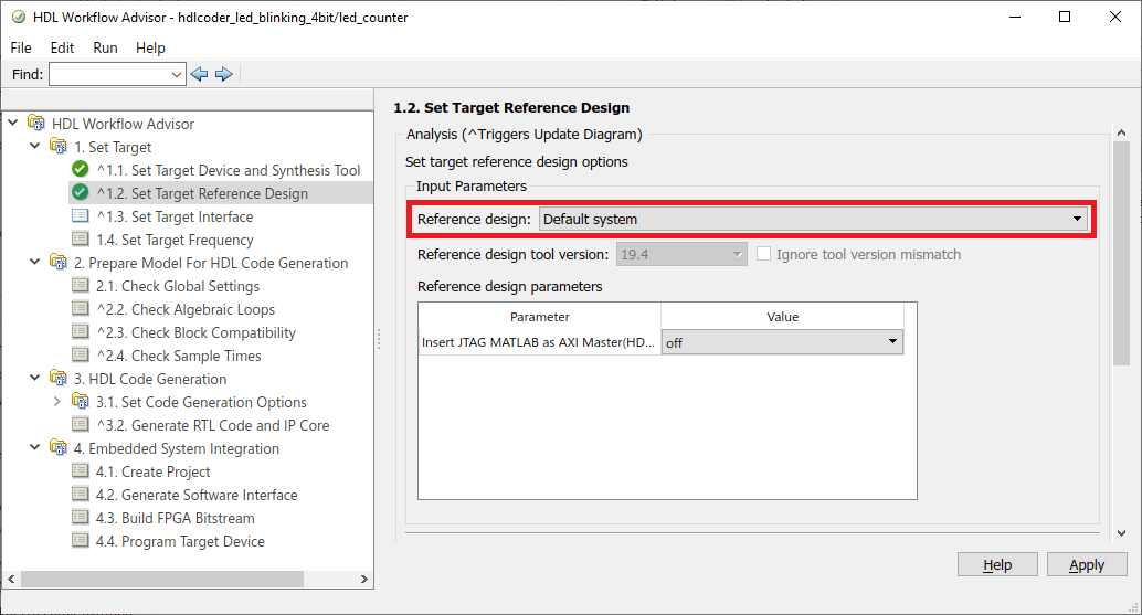
In task 1.2 Set Target Reference Design, select
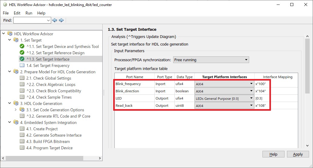
Default system.In task 1.3 Set Target Interface, map the ports:
Set Blink_frequency, Blink_direction, and Read_back to
AXI4.Set LED to
LEDs General Purpose [0:3].
Map each port in your DUT to one of the IP core target interfaces. In this example:
The input ports Blink_frequency and Blink_direction are mapped to the
AXI4interface, so HDL Coder generates AXI interface accessible registers for them.The LED output port is mapped to an external interface,
LEDs General Purpose [0:3], which connects to the LED hardware on the Intel SoC board.
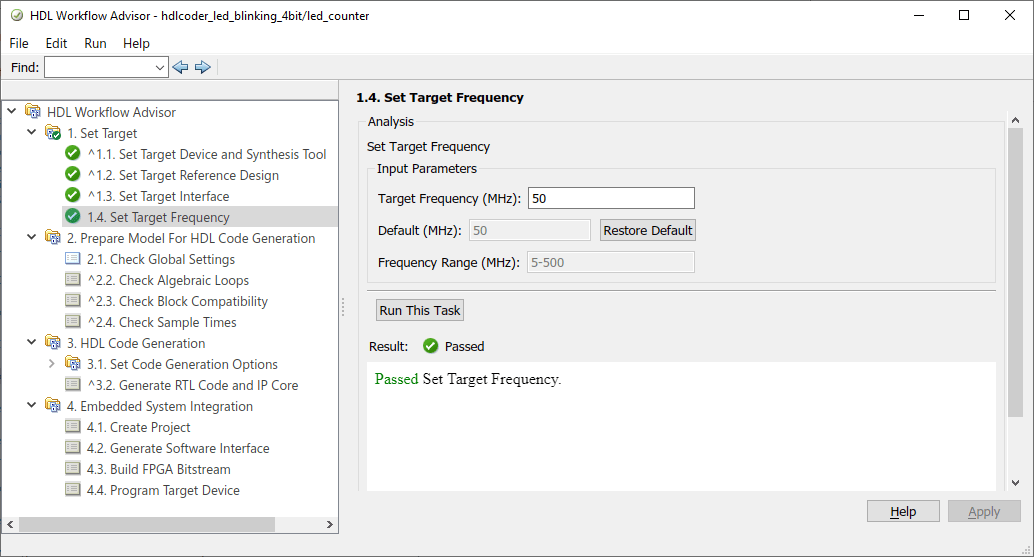
In task 1.4 Set Target Frequency, set the Target Frequency to
50 MHz.
Registers mapped to the DUT inports Blink_frequency, Blink_direction are write registers.
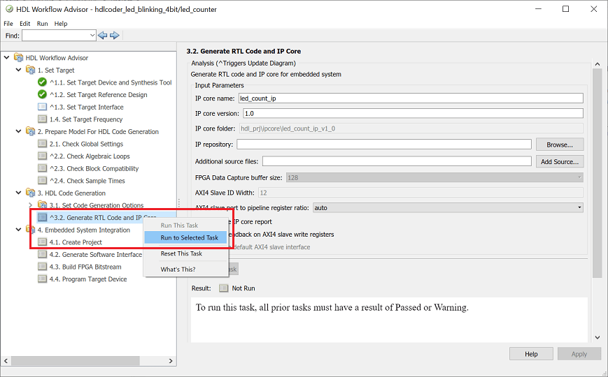
Generate the IP Core
To read values stored in these registers by using
devmem, in task 3.2 Generate RTL Code and IP Core, select the Enable readback on write registers.Right-click task 3.2 Generate RTL Code and IP Core and select Run to selected task to generate the IP Core for your Simulink design.
After you generate the custom IP core, the IP core files are in the ipcore folder within your project folder. Open the Code Generation Report HTML file and review the IP Core Generation Report section to see the register address mapping for DUT ports. For more information, see Custom IP Core Report.
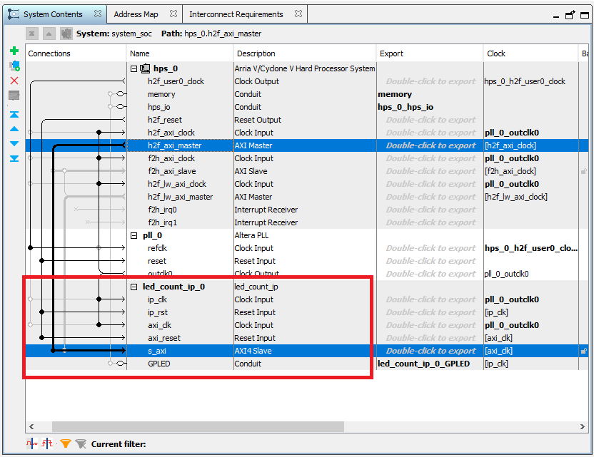
Integrate Generated IP Core into the Qsys Environment
To integrate the generated HDL IP Core into your reference design:
Run task 4.1 Create Project.
After the task completes, click the link in the Result pane to view the generated Quartus Pro project.
In Quartus Pro, launch Platform Designer. The reference design shows the project architecture.
Generate the Software Interface Model
In the HDL Workflow Advisor, click task 4.2 Generate Software Interface. Select Generate Simulink software interface model and Generate host interface script and click Run the task.
When the task completes, the HDL Workflow Advisor generates the
gm_hdlcoder_led_blinking_4bit_interface.slx. Save this model in your working directory. It also generates thegs_hdlcoder_led_blinking_4bit_interface.mandgs_hdlcoder_led_blinking_4bit_setup.mscripts in your working directory.
Build and Program the Bitstream
To generate the bitstream, run task 4.3 Build FPGA Bitstream.
To load the bitstream file on the hardware board, run task 4.4 Program Target Device.
After you load the bitstream, the LEDs on the Arria 10 SoC board start blinking.
Verify the Design
Control the LED blink frequency and direction by running the generated software interface model. For details on using the software interface model, see Get Started with IP Core Generation for Intel SoC Devices.