Reference Designs for RFSoC Devices
HDL Coder™ or SoC Blockset™ provides the following reference designs for the supported RFSoC devices. Use these reference designs with the IP core generation workflow.
Default system— This is a basic reference design that supports data steaming between the processor and the FPGA. It also provides access to the PL-DDR4 memory. This reference design does not include the RF Data Converter IP and therefore does not include the digital-to-analog converter (DAC) and analog-to-digital converter (ADC) real or in-phase/quadrature (I/Q) interfaces.Real ADC/DAC Interface— This design receives and transmits real data and supports DAC and ADC real-time ports.IQ ADC/DAC Interface— This design receives and transmits complex I/Q data and supports DAC and ADC real-time ports.Deep Learning design with real DAC/ADC interface— This design receives and transmits real data and supports DAC and ADC real-time ports. This deep learning reference design enables you to preprocess the received data, send the preprocessed data to the memory, and the deep learning processor processes the data.Deep Learning design with IQ DAC/ADC interface— This design receives and transmits complex I/Q data and supports DAC and ADC real-time ports. This deep learning reference design enables you to preprocess the received data, send the preprocessed data to the memory, and the deep learning processor processes the data.
Add an RF Data Converter block to your Simulink® model to use these functionalities of the RFSoC reference designs:
Real-time NCO ports for DAC and ADC
Real-time ports for ADC
External PLL
Different parameter values for each selected DAC and ADC
Generate an IP core for a design under test (DUT) and integrate the generated IP core into these reference designs. Connect the IP core with rest of the design by using the AXI4-Stream Master, AXI4-Stream Slave, AXI4 Master, interrupt, AXI4-Lite, and DAC and ADC real or I/Q interfaces. The figure shows how the interfaces connect the processor to the DUT:
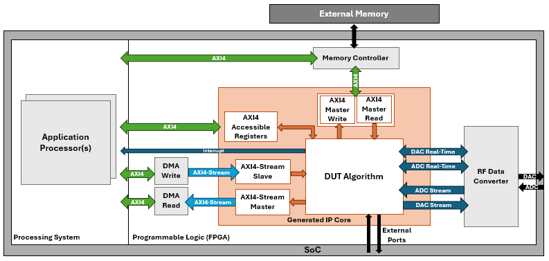
HDL Coder generates the HDL IP core for the DUT and inserts it into the RFSoC reference design. The RFSoC reference design includes a processor and the generated IP core. The processor acts as a manager and the IP core acts as a subordinate. By accessing the generated registers via the AXI4-Lite interface, the processor can read and write data to and from the IP core.
The RFSoC reference design includes a direct memory access (DMA) IP to handle the data streaming between the processor and the IP core. The DMA controller acts as both a manager and a subordinate. The AXI4-Stream interfaces process the data stream from the DMA controller and send the output data stream back to the DMA controller.
The IP core reads the input data from the external memory via the AXI4 Master interface. The IP core then computes the algorithm and writes the result to external memory via the AXI4 Master interface. The processor can read the result from memory and then verify it in MATLAB®.
You can tune the parameters on the FPGA, or probe the results from the FPGA via the
AXI4-Lite interface in the IP core. To tune the parameters or probe results, use this
reference design with External mode in Simulink.
Supported Interface Methods
You can use the RFSoC reference designs with these interfaces:
Register Interface (AXI4-Lite or AXI4) — Use this interface to access the control and status registers in your design. You can choose between AXI4-Lite or AXI4 protocol for the register interface. Use AXI4-Lite if you need only lightweight data transfers. Use AXI4 to connect to components that support burst data transfers. For more information, see Register Interface (AXI4-Lite/AXI4) (HDL Coder).
AXI4 Master — Use this interface for designs that require you to access memory, or to control other IP cores with AXI4 or AXI4-Lite interfaces. Example applications include moving large amounts of data between your algorithm and external DDR memory. For more information, see AXI4 Master (HDL Coder).
AXI4-Stream — Use this interface for moving streaming data or transferring data at high speeds. Example applications include transferring large amounts of data between processors and FPGAs using DMA. For more information, see AXI4-Stream (HDL Coder).
External I/O and External Port — Use this interface to connect to peripherals on your hardware board, such as LEDs, push buttons, DIP switches, FPGA pins, and so on. For more information, see External I/O and External Port (HDL Coder).
FPGA Data Capture — Use this interface to capture raw data from outputs or signals by using test points in your design and then use the data to debug your design. For more information, see FPGA Data Capture (HDL Coder).
Interrupt — Use this interface to send interrupt signal from DUT to processor to trigger an event-driven task.
DAC and ADC Stream — Use this interface to transmit and receive real or complex I/Q data between the DUT and the RF Data Converter IP, based on the selected reference design.
DAC and ADC Real-Time — Use this interface to connect the DUT to the DAC and ADC real-time ports of the RF Data Converter IP. This interface is available only if you have an RF Data Converter block in your model.
Supported Boards
You can use the RFSoC reference design architectures with these target platforms:
Xilinx® Zynq® UltraScale+™ RFSoC ZCU111 Evaluation Kit
Xilinx Zynq UltraScale+ RFSoC ZCU208 Evaluation Kit
Xilinx Zynq UltraScale+ RFSoC ZCU216 Evaluation Kit
Xilinx Zynq UltraScale+ RFSoC DFE ZCU670 Evaluation Kit
Note
The deep learning reference designs are not supported for the ZCU670 evaluation kit.
Target Algorithm to Reference Design
To target your algorithm in Simulink to the RFSoC reference design:
Model your algorithm.
On the HDL Code tab of the Simulink toolstrip, in the Output section, set the drop-down button to IP Core.
Select your DUT and make sure that Code for is set to this DUT.
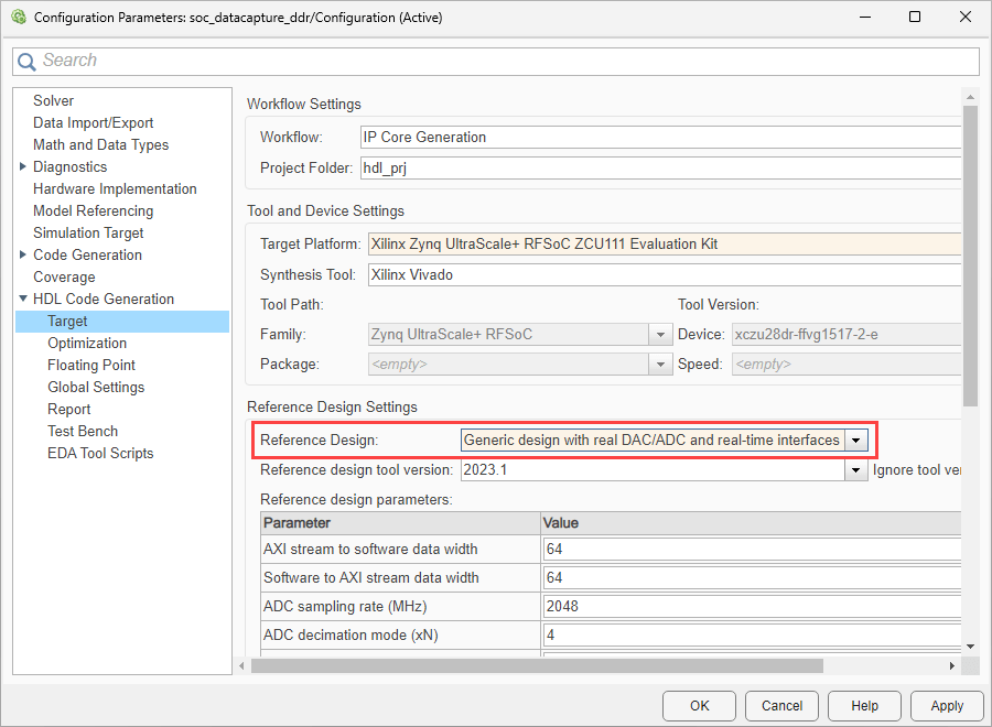
Open the HDL Code Generation > Target tab of the Configuration Parameters dialog box by clicking the Settings button.
Set Workflow to
IP Core Generation.Set Target Platform to a supported hardware board listed in Supported Boards. Ensure that Synthesis Tool is set to
Xilinx Vivado.Set Reference Design to an option that best matches your requirements.
Alternatively, you can also set the target reference design by using the HDL Workflow Advisor tool. Follow these steps in the HDL Workflow Advisor.
In the 1.1. Set Target Device and Synthesis Tool step, set Target workflow to
IP Core
                            Generation
. Set Target platform to a supported hardware board listed in Supported Boards. Ensure that Synthesis tool is set toXilinx Vivado.In the 1.2. Set Target Reference Design step, set Reference design to an option that best matches your requirements.

Go through the workflow to generate the HDL IP core, and integrate the IP core into the selected reference design.
Set Reference Design Parameters
In the Configuration Parameters dialog box, on the HDL Code Generation > Target tab, set reference design parameters to the required values.
Note
If your model includes an RF Data Converter block, the code generation process uses all the parameter values you specify in the block. If the model does not include this block, the process uses the reference design parameters for code generation.
Default System Reference Design Parameters
The Default system reference design has these configuration
parameters:
Add stream to software (AXI4-Stream Master)
Add the AXI4-Stream Master interface to the reference design by setting this parameter to
true.Add stream from software (AXI4-Stream Slave)
Add the AXI4-Stream Slave interface to the reference design by setting this parameter to
true.Add external memory access (AXI4 Master)
Add access to external memory via the AXI4 Master interface by setting this parameter to
true.AXI4-Stream Master data width
Specify the data width for the AXI4-Stream Master interface as 32, 64, or 128 bits.
AXI4-Stream Slave data width
Specify the data width for the AXI4-Stream Slave interface as 32, 64, or 128 bits.
FPGA Data Capture (HDL Verifier required)
Generate and integrate the data capture IP into the reference design. Use FPGA data capture to observe signals from your design while the design is running on the FPGA. This feature captures a window of signal data from the FPGA and returns the data to MATLAB or Simulink over a JTAG connection. To capture data over a JTAG connection, set this parameter to
JTAG. To capture data over an Ethernet connection, set this parameter toPL Ethernet. Then, map each signal that you want to capture to theFPGA Data Captureinterface.Note
FPGA data capture in Configuration Parameters support programmable logic (PL) Ethernet only. The processing system (PS) Ethernet is not supported.
To enable the
PL Ethernetoption for the Xilinx boards that have the Ethernet physical layer (PHY), manually add the Ethernet media access controller (MAC) Hub IP in theplugin_boardfile using theaddEthernetMACInterface(HDL Coder) method before you open the Configuration Parameters dialog box.FPGA data capture in Configuration Parameters does not support SGMII interface.
Real and I/Q ADC/DAC and Deep Learning Reference Designs Parameters
The Real ADC/DAC Interface, IQ ADC/DAC
Interface, Deep Learning design with real DAC/ADC
interface, and Deep Learning design with IQ DAC/ADC
interface reference designs have these configuration
parameters:
AXI4-Stream Master data width
Specify the data width for the AXI4-Stream Master interface as 32, 64, or 128 bits.
AXI4-Stream Slave data width
Specify the data width for the AXI4-Stream Slave interface as 32, 64, or 128 bits.
Add external memory access (AXI4 Master)
Add access to external memory via the AXI4 Master interface by setting this parameter to
true.ADC sampling rate (MHz)
Specify the sampling rate for ADC as a scalar in a range that is based on the selected hardware board. This table shows the ADC sampling rate range for the supported RFSoC devices.
RFSoC Device Hardware Board Sampling Rate Range (MHz) ZU28DR
Zynq UltraScale+ RFSoC ZCU111 Evaluation Kit
[1000, 4096] ZU48DR
Zynq UltraScale+ RFSoC ZCU208 Evaluation Kit
[1000, 5000] ZU49DR
Zynq UltraScale+ RFSoC ZCU216 Evaluation Kit
[500, 2500] ZU67DR
Zynq UltraScale+ RFSoC DFE ZCU670 Evaluation Kit
[500, 2950] — For quad ADC tiles
[1000, 5900] — For dual ADC tiles
ADC decimation mode (xN)
Specify the decimation factor. The ZCU111 RFSoC device supports decimation factors of 1, 2, 4, and 8. The ZCU208, ZCU216, and ZCU670 RFSoC devices support decimation factors of 1, 2, 3, 4, 5, 6, 8, 10, 12, 16, 20, 24, and 40.
ADC samples per clock cycle
Specify the number of samples per clock cycle for ADC as an integer from 1 to 16. The supported values for the number of samples per clock cycle vary with the selected hardware board and reference design.
The ADC stream data width is: 16 x ADC samples per clock cycle.
The ADC stream clock frequency is: ADC sampling rate (MHz) / ADC decimation mode (xN) x ADC samples per clock cycle.
ADC mixer type
Specify the mixer type for ADC as
Bypassed,Coarse, orFine. TheReal ADC/DAC InterfaceandDeep Learning design with real DAC/ADC interfacereference designs supportBypassedmixer type. TheIQ ADC/DAC InterfaceandDeep Learning design with IQ DAC/ADC interfacereference designs supportCoarseandFinemixer types.DAC sampling rate (MHz)
Specify the sampling rate for DAC as a scalar in a range that is based on the selected hardware board. This table shows the DAC sampling rate range for the supported RFSoC devices.
RFSoC Device Hardware Board Sampling Rate Range (MHz) ZU28DR
Zynq UltraScale+ RFSoC ZCU111 Evaluation Kit
[500, 6554] ZU48DR
Zynq UltraScale+ RFSoC ZCU208 Evaluation Kit
[500, 7000] ZU49DR
Zynq UltraScale+ RFSoC ZCU216 Evaluation Kit
ZU67DR
Zynq UltraScale+ RFSoC DFE ZCU670 Evaluation Kit
DAC interpolation mode (xN)
Specify the interpolation factor. The ZCU111 RFSoC device supports interpolation factors of 1, 2, 4, and 8. The ZCU208, ZCU216, and ZCU670 RFSoC devices support interpolation factors of 1, 2, 3, 4, 5, 6, 8, 10, 12, 16, 20, 24, and 40.
DAC samples per clock cycle
Specify the number of samples per clock cycle for DAC as an integer from 1 to 16. The supported values for the number of samples per clock cycle vary with the selected hardware board and reference design.
The DAC stream data width is: 16 x DAC samples per clock cycle.
The DAC stream clock frequency is: DAC sampling rate (MHz) / DAC interpolation mode (xN) x DAC samples per clock cycle.
DAC mixer type
Specify the mixer type for DAC as
Bypassed,Coarse, orFine. TheReal ADC/DAC InterfaceandDeep Learning design with real DAC/ADC interfacereference designs supportBypassedmixer type. TheIQ ADC/DAC InterfaceandDeep Learning design with IQ DAC/ADC interfacereference designs supportCoarseandFinemixer types.ADC/DAC NCO mixer LO (GHz)
Specify the NCO mixer frequency values as a scalar. The value of this parameter is valid only when you set ADC Mixer type and DAC Mixer type to
Fine.Dependencies
To enable this parameter, set Reference Design to
IQ ADC/DAC InterfaceorDeep Learning design with IQ DAC/ADC interface.Enable multi-tile sync
Enable multi-tile synchronization (MTS) by setting this parameter to
true. For more information about MTS, see Multi tile sync.Tile clock output frequency (MHz)
This parameter is read-only. It shows the frequency of the clock generated by the ADC tile. The reference design uses this frequency as an input to generate the required clock for the DUT. The ADC sampling rate derives the value of this parameter.
DUT synthesis frequency (MHz)
This parameter is read-only. It shows the frequency of the clock that drives the DUT. The DAC or ADC sampling rate, interpolation or decimation factor, and DAC or ADC samples per clock cycle derive the value of this parameter.
PLL reference clock (MHz)
This parameter is read-only. It shows the frequency of the input reference clock to the internal PLL in the DAC or ADC tile.
FPGA Data Capture (HDL Verifier required)
Generate and integrate the data capture IP into the reference design. Use FPGA data capture to observe signals from your design while the design is running on the FPGA. This feature captures a window of signal data from the FPGA and returns the data to MATLAB or Simulink over a JTAG connection. To capture data over a JTAG connection, set this parameter to
JTAG. To capture data over an Ethernet connection, set this parameter toPL Ethernet. Then, map each signal that you want to capture to theFPGA Data Captureinterface.Note
FPGA data capture in Configuration Parameters support programmable logic (PL) Ethernet only. The processing system (PS) Ethernet is not supported.
To enable the
PL Ethernetoption for the Xilinx boards that have the Ethernet physical layer (PHY), manually add the Ethernet media access controller (MAC) Hub IP in theplugin_boardfile using theaddEthernetMACInterface(HDL Coder) method before you open the Configuration Parameters dialog box.FPGA data capture in Configuration Parameters does not support SGMII interface.
The deep learning RFSoC reference designs have these additional parameters:
DL Processor IP Name
This parameter is always
dlprocessorunless the packing of the IP is changed.DL Processor IP Location
This parameter shows the location of the
dlprocessorwhere the IP is available.DL Processor IP Vendor
This parameter depends on the license of the Vivado® tool where DL HDL IP is generated.
Map DUT Ports
To automatically map the DUT ports to the required interfaces, on the System on Chip tab, click Map Interfaces.
You can view and edit the interface mapping by following these steps:
On the HDL Code tab, click Target Interface to open the IP Core editor.
Select the Interface Mapping tab to map each DUT port to one of the IP core target interfaces. If no mapping table appears, click the Reload IP core settings
 button to compile the model and repopulate the
DUT ports and their data types.
button to compile the model and repopulate the
DUT ports and their data types.Validate your settings by clicking the Validate IP core settings
 button.
Generate IP Core and Program FPGA
Generate the IP core and the FPGA bitstream file. Then, program the FPGA by following these steps:
In the Simulink toolstrip, on the HDL Code tab, click Build Bitstream to generate the IP core and bitstream file. Wait until the synthesis tool runs in the external window.
Expand the Build Bitstream menu. Then, select Program Target Device to download the bitstream.
Generate Host Interface Script
Verify the generated IP core on the hardware board by using the generated host interface script. This script contains the DUT ports and interface mapping information. Use this script to access the board memory, DUT registers, and AXI4-Stream interfaces from MATLAB. To generate a host interface script file, in the Simulink toolstrip, on the HDL Code tab, expand the Host Interface Script menu. Then, select Host Interface Script. This option generates these MATLAB files:
gs_modelName_setup— This script adds the AXI4 Slave, AXI4-Stream, and memory interfaces. The script also contains DUT port objects that contain the port name, direction, data type, and interface mapping information. The script then maps the DUT ports to the corresponding interfaces.gs_modelName_interface— This script creates a target object, instantiates the setup scriptgs_modelName_setup, and then connects to the target hardware. The script then sends read and write commands to the generated HDL IP core.
For more information about host interface script, see Host Interface Script Files (HDL Coder).
Generate Software Interface Model
To target your hardware board, you can generate a software model in addition to the FPGA model. This action generates two models: a hardware interface model and a software interface model. It also generates two libraries that contain the interface blocks used in the generated models.
The software interface model and its library are generated only if you have Embedded Coder®, SoC Blockset, and SoC Blockset Support Package for AMD FPGA and SoC Devices installed.
You can use the hardware interface model to control the reference design on the board, including IP core, from the Simulink model, without Embedded Coder.
The software interface model enables you to target your software algorithms to the ARM® processor on the board.
For more information about software interface model, see Generate SoC Software Model.