Four-Quadrant Chopper
Controller-driven four quadrant DC-DC chopper
Libraries:
Simscape /
Electrical /
Semiconductors & Converters /
Converters
Description
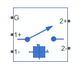
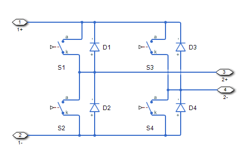
The Four-Quadrant Chopper block represents a four-quadrant controlled chopper for converting a fixed DC input to a variable DC output. The block contains two bridge arms. Each bridge arm each has two switching devices.
You can choose from two fidelity levels for the converter model. The equivalent model
option does not model the individual switching devices but returns equivalent results.
If you need detailed results for the switching device dynamics, use the detailed model
option. Otherwise, use the equivalent model for faster simulation. To simulate in real
time, use the equivalent model. To validate the results, use the detailed model with a
variable-step solver. To use the detailed model, set the Fidelity
level parameter to Detailed model - switching
devices. To use the equivalent model, set the Fidelity
level parameter to Equivalent model -
PWM-controlled.
If you choose the detailed model, each component is the same switching device, which you specify by setting the Switching device parameter. The switching devices that you can specify are implementations of blocks in the Simscape > Electrical > Semiconductors & Converters library:
GTO — Gate turn-off thyristor. For information about the I-V characteristic of the device, see GTO.
Ideal semiconductor switch — For information about the I-V characteristic of the device, see Ideal Semiconductor Switch.
IGBT — Insulated-gate bipolar transistor. For information about the I-V characteristic of the device, see IGBT (Ideal, Switching).
MOSFET — N-channel metal-oxide-semiconductor field-effect transistor. For information about the I-V characteristic of the device, see MOSFET (Ideal, Switching).
Thyristor — For information about the I-V characteristic of the device, see Thyristor (Piecewise Linear).
Averaged Switch — Semiconductor switch with an antiparallel diode. The control signal port G accepts values in the interval [0,1]. When G is equal to
0or1, the averaged switch is fully opened or fully closed respectively. The switch behaves similarly to the Ideal Semiconductor Switch block with an antiparallel diode. When G is between 0 and 1, the averaged switch is partly opened. You can average the pulse-width modulation (PWM) signal over a specified period. You can then undersample the model or use modulation waveforms instead of PWM signals.
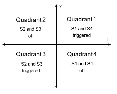
The figures show the equivalent circuit and the operation for the block.
To use the equivalent model as a rectifier, set all the elements of the PWM signal to zero. The model behaves as a diode rectifier.
Protection
The block contains an integral protection diode for each switching device. The integral diode protects the semiconductor device by providing a conduction path for reverse current. An inductive load can produce a high reverse-voltage spike when the semiconductor device suddenly switches off the voltage supply to the load.
To configure the internal protection diode block, use the Protection Diode parameters. This table shows how to set the Model dynamics parameter based on your goals.
| Goals | Value to Select | Integral Protection Diode | |
|---|---|---|---|
| Do not include protection. | None | None | |
| Include protection. | Prioritize simulation speed. | Diode with no dynamics | The Diode block |
| Prioritize model fidelity by precisely specifying reverse-mode charge dynamics. | Diode with charge dynamics | The dynamic model of the Diode block | |
Note
If you set the Switching device parameter to
Averaged Switch, the block automatically models
protection diodes with no dynamics and the Model dynamics
parameter is not visible.
You can also include a snubber circuit for each switching device. Snubber circuits contain a series-connected resistor and capacitor. They protect switching devices against high voltages that inductive loads produce when the device turns off the voltage supply to the load. Snubber circuits also prevent excessive rates of current change when a switching device turns on.
To include and configure a snubber circuit for each switching device, use the Snubbers parameters.
Modeling Thermal Effects
Since R2024b
You can expose the thermal port to model the effects of generated heat and device temperature. To expose the thermal port:
In the Main settings, set the Fidelity level parameter to
Detailed model - switching devices.In the Switching Devices settings, set the Switching device parameter to one of these options:
GTOIGBTMOSFETThyristor
In the Switching Devices settings, select the Model thermal effects parameter.
For more information on using thermal ports and the Thermal Port parameters, see Simulating Thermal Effects in Semiconductors.
When you expose the thermal port, the Four-Quadrant Chopper block models the conduction losses and
the turn-on and turn-off losses of the switching devices. The block uses the same
methods to calculate these losses as these blocks with the On-state
behavior and switching losses parameter set to Specify
constant values:
For more information about how the Four-Quadrant Chopper block calculates these losses, see the documentation for the block that matches the option you select for the Switching device parameter.
If you enable the thermal port and you set the Integral protection
diode parameter to Diode with no dynamics,
the block also models reverse recovery loss for the protection diodes. The block
uses the same method to calculate these losses as the Diode block with the Fidelity level
parameter set to Ideal switching and the Diode
model parameter to Piecewise
linear.
With ideal switching, the block does not use a physics-based charge model. The block represents the losses that the charge creates during reverse recovery as an instantaneous loss.
The block applies reverse recovery losses by stepping up the junction temperature with a value equal to the reverse recovery loss divided by the total thermal mass at the junction.
If you set the Reverse recovery loss model
parameter to Tabulated loss, the value of the
Reverse recovery loss table, Erec(Tj, If) parameter
specifies the dissipated energy as a function of the junction temperature and the
forward current just before the switching event. The off-state voltage linearly
scales the losses relative to the Turn-off voltage when measuring recovery
loss, Vrec parameter value. The table uses delayed values for the
current and voltage. To use a value in the lookup table that is close to the
instantaneous value, set the Filter time constant for voltage
and current values parameter to a value that is lower than the
fastest switching period.
If you set the Reverse recovery loss model
parameter to Fixed loss, the value of the
Reverse recovery loss parameter specifies the energy
dissipated during each turn-off event. If you select the Scale reverse
recovery loss with current and voltage parameter, then the block
scales this loss value linearly by the on-state current and the off-state voltage.
To use scaling values that are close to the instantaneous values, set Filter time constant for voltage and current values to a
value that is lower than the fastest switching period.
Gate Control
To connect Simulink® gate-control voltage signals to the gate ports of the internal switching devices:
Convert each voltage signal using a Simulink-PS Converter block.
Multiplex the converted gate signals into a single vector using a Four-Pulse Gate Multiplexer block.
Connect the vector signal to the G port.
Piecewise Constant Approximation in Averaged Switch for FPGA Deployment
If you set the Switching device parameter to Averaged switch and your model uses a partitioning solver, this block produces nonlinear partitions because the average mode equations include modes, Gsat that are functions of the input G. To make these equations compatible with hardware description language (HDL) code generation, and therefore FPGA deployment, set the Integer for piecewise constant approximation of gate input (0 for disabled) parameter to a value greater than 0. This block then treats the Gsat mode as a piecewise constant integer with a fixed range. This turns the previously nonlinear partitions to linear time varying partitions.
An integer value in the range [0,K], where K is the value of the Integer for piecewise constant approximation of gate input (0 for disabled), is now associated with each real value mode in the range [0,1]. The block computes the piecewise constant mode by dividing the original mode by K to normalize it back to the range [0,1]:
Examples
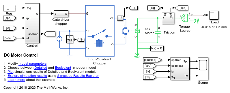
DC Motor Control
A cascade speed-control structure for a DC motor. A PWM controlled four-quadrant Chopper is used to feed the DC motor. The Control subsystem includes the outer speed-control loop, the inner current-control loop, and the PWM generation. The total simulation time (t) is 4 seconds. At t = 1.5 seconds, the load torque increases. At t = 2.5 seconds, the reference speed is changed from 1000 rpm to 2000 rpm.
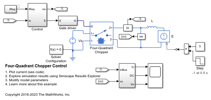
Four-Quadrant Chopper Control
Control a four-quadrant chopper. The Control subsystem implements a simple PI-based control algorithm for controlling the output current. The simulation uses both positive and negative references. The total simulation time (t) is 1 second. At t = 0.5 seconds, the polarity of the load DC source E is changed.
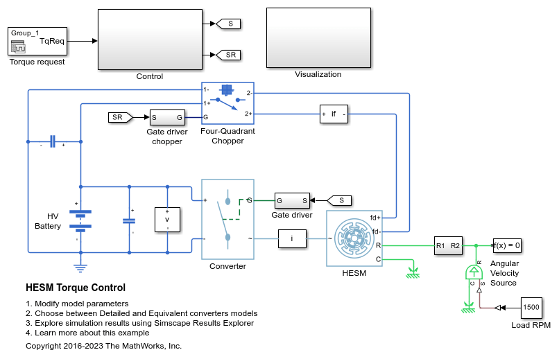
HESM Torque Control
Control the torque in a hybrid excitation synchronous machine (HESM) based electrical-traction drive. Permanent magnets and an excitation winding excite the HESM. A high-voltage battery feeds the SM through a controlled three-phase converter for the stator windings and through a controlled four quadrant chopper for the rotor winding. An ideal angular velocity source provides the load. The Control subsystem uses an open-loop approach to control the torque and a closed-loop approach to control the current. At each sample instant, the torque request is converted to relevant current references. The current control is PI-based. The simulation uses several torque steps in both the motor and generator modes. The Visualization subsystem contains scopes that allow you to see the simulation results.
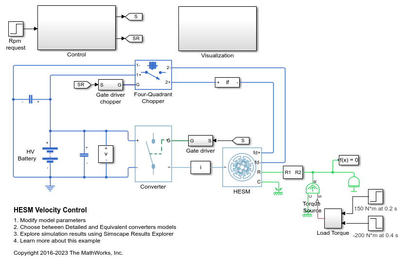
HESM Velocity Control
Control the rotor angular velocity in a hybrid excitation synchronous machine (HESM) based electrical-traction drive. Permanent magnets and an excitation winding excite the HESM. A high-voltage battery feeds the HESM through a controlled three-phase converter for the stator windings and through a controlled four quadrant chopper for the rotor winding. An ideal torque source provides the load. The Control subsystem includes a multi-rate PI-based cascade control structure. The control structure has an outer angular-velocity-control loop and three inner current-control loops. The Visualization subsystem contains scopes that allow you to see the simulation results.
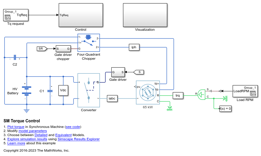
SM Torque Control
Control the torque in a synchronous machine (SM) based electrical-traction drive. A high-voltage battery feeds the SM through a controlled three-phase converter for the stator windings and a controlled four quadrant chopper for the rotor winding. An ideal angular velocity source provides the load. The Control subsystem uses an open-loop approach to control the torque and a closed-loop approach to control the current. At each sample instant, the torque request is converted to relevant current references. The current control is PI-based. The simulation uses several torque steps in both motor and generator modes. The task scheduling is implemented as a Stateflow® state machine. The Visualization subsystem contains scopes that allow you to see the simulation results.
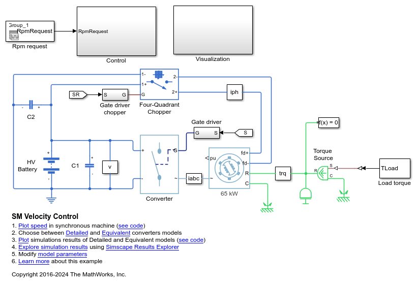
SM Velocity Control
Control the rotor angular velocity in a synchronous machine (SM) based electrical-traction drive. A high-voltage battery feeds the SM through a controlled three-phase converter for the stator windings and a controlled four quadrant chopper for the rotor winding. An ideal torque source provides the load. The Control subsystem includes a multi-rate PI-based cascade control structure which has an outer angular-velocity-control loop and three inner current-control loops. The task scheduling in the Control subsystem is implemented as a Stateflow® state machine. The Visualization subsystem contains scopes that allow you to see the simulation results.
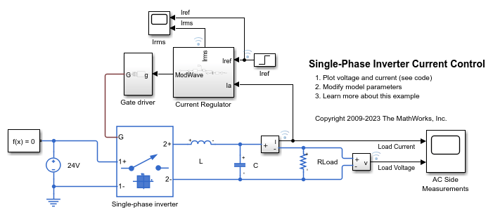
Single-Phase Inverter Current Control
Control the current in a single-phase inverter system. The single-phase inverter uses averaged switches fed by modulation waveforms. This example is suitable for real-time evaluation on a dedicated real-time emulator.
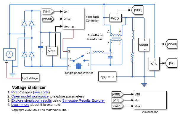
Power Converter Voltage Stabilizer
A voltage stabilizer circuit. It uses a full-wave rectifier, a single-wave inverter, and a buck-boost transformer to achieve voltage regulation.

Compare Fidelity Levels of Chopper Converters
Use different levels of fidelity in chopper converters. You change the level of fidelity by changing the values for the Fidelity level, Switching device, and Integral protection diode parameters of the Four-Quadrant Chopper block. You also change the inputs to the G port. Using a higher level of fidelity improves the accuracy of the results but it also slows down simulation.
Assumptions and Limitations
If, in the Solver Configuration block inside your model, you set the Solver type parameter to
Partitioning, the averaged switches introduce instability during dead time, when all gate inputs are set to 0. Where possible, use the open-zero state by setting all high-side switches to 0 and all low-side switches to 1.If you use the block as a rectifier and you set the Fidelity level parameter to
Equivalent model - PWM-controlled, the AC voltage must originate from an ideal active source, not a passive one like a mutual inductor.
Ports
Conserving
Parameters
References
[1] Trzynadlowski, A. M. Introduction to Modern Power Electronics, 2nd Edition. Hoboken, NJ: John Wiley & Sons Inc., 2010.