Custom Geometry and PCB Fabrication
Use the shape objects to create different designs and complex shapes and create custom printed circuit board (PCB) components to complete PCB designs quickly. Use line interconnects such as bends, curves, mitered edges, and traces to effectively lay out PCB components.
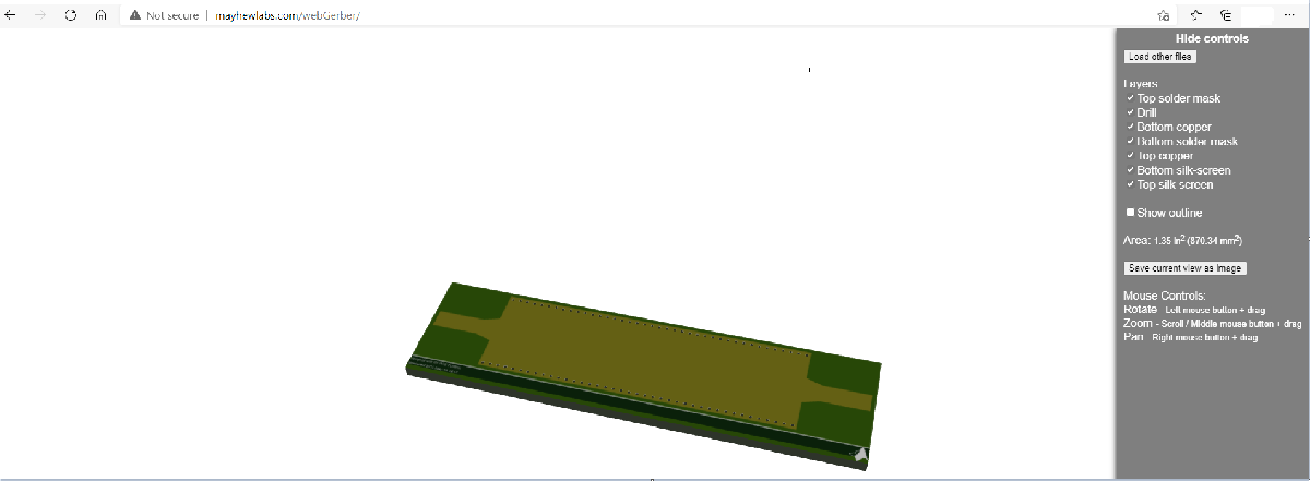
Gerber files are open ASCII vector format files that contain information on each physical board layer of the PCB design. These files also represent circuit board objects, like copper traces, vias, pads, solder mask, and silkscreen images by series of coordinates. Write Gerber files that can be used by PCB manufacturers to translate the details of the design into physical properties of the PCB.
Apps
| PCB VIEWER | Import, visualize, inspect, and navigate printed circuit boards (Since R2026a) |
Objects
Functions
Topics
- Board Thickness versus Dielectric Thickness in PCB
This example shows you how to define the BoardThickness of PCB with respect to dielectric thickness of
pcbComponentobject for different use-cases.
